Third-generation semiconductor contact window structure and manufacturing method thereof

A manufacturing method and contact window technology, which is applied in semiconductor/solid-state device manufacturing, semiconductor devices, semiconductor/solid-state device components, etc., can solve problems such as lattice structure damage, high contact window resistance, impurity ion pollution, etc., to achieve improved Anti-acid corrosion, reduce contact resistance, and reduce the effect of process steps

Pending Publication Date: 2022-05-27
GALLIUM ADVANCE SEMICON TECH CO
View PDF0 Cites 0 Cited by
  • Summary
  • Abstract
  • Description
  • Claims
  • Application Information

AI Technical Summary

Problems solved by technology

[0003] The main purpose of the present invention is to provide a third-generation semiconductor contact window structure and its manufacturing method, aiming to solve the lattice structure damage and impurity ion pollution on the surface of the compound epitaxial layer caused by the metal sputtering process of the third-generation semiconductor device, and Technical problem of high contact window resistance

Method used


Image

  • Third-generation semiconductor contact window structure and manufacturing method thereof
  • Third-generation semiconductor contact window structure and manufacturing method thereof
  • Third-generation semiconductor contact window structure and manufacturing method thereof

Examples


Embodiment Construction

[0029] In order to facilitate the understanding of the present invention, the present invention will be described in more detail below with reference to the accompanying drawings and specific embodiments. It should be noted that when an element is referred to as being "fixed to" another element, it can be directly on the other element, or one or more intervening elements may be present therebetween. When an element is referred to as being "connected" to another element, it can be directly connected to the other element or one or more intervening elements may be present therebetween. The terms "vertical", "horizontal", "left", "right", "inner", "outer" and similar expressions used in this specification are for illustrative purposes only. In the description of the present invention, the terms "first" and "second" are only used for descriptive purposes, and cannot be understood as indicating relative importance, or implicitly indicating the number of indicated technical features....


PUM

PropertyMeasurementUnit
angleaaaaaaaaaa

Abstract

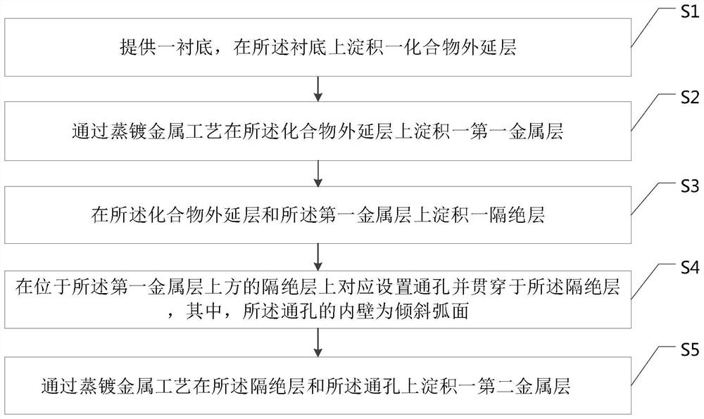
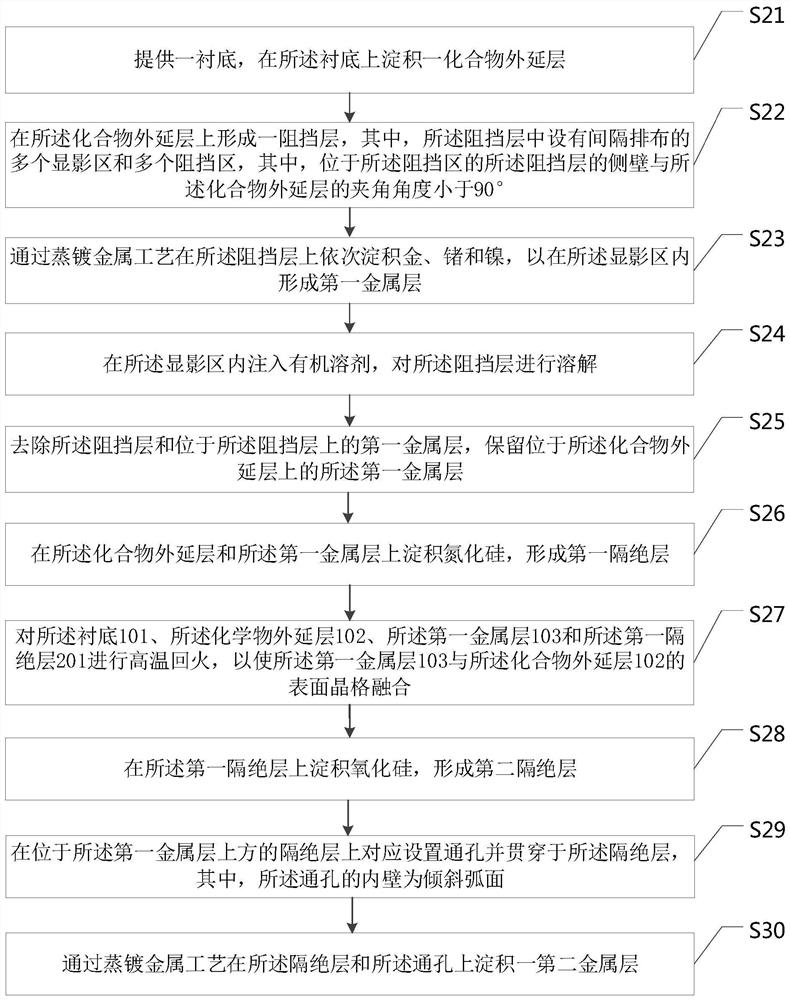
The invention relates to the technical field of semiconductor manufacturing, and discloses a third-generation semiconductor contact window structure and a manufacturing method thereof. The manufacturing method comprises the following steps: providing a substrate, and depositing a compound epitaxial layer on the substrate; depositing a first metal layer on the compound epitaxial layer through a metal evaporation process; depositing an isolation layer on the compound epitaxial layer and the first metal layer; a through hole is correspondingly formed in the portion, located above the first metal layer, of the isolation layer and penetrates through the isolation layer, and the inner wall of the through hole is an inclined cambered surface; and depositing a second metal layer on the isolation layer and the through hole through a metal evaporation process. Damage and impurity ion pollution to a lattice structure on the surface of a compound epitaxial layer by a metal sputtering process are effectively prevented, and the contact impedance of a third-generation semiconductor contact window structure is reduced.

Description

technical field [0001] The present invention relates to the technical field of semiconductor manufacturing, in particular to a third-generation semiconductor contact window structure and a manufacturing method thereof. Background technique [0002] In the traditional compound semiconductor manufacturing industry, an insulating layer is usually deposited on the surface of the compound, and then holes are opened in a fixed area through photolithography and etching processes, and then metal is deposited in the through holes to form through-hole metal and metal wiring. There are the following drawbacks: 1. Performing the etching process directly on the surface of the compound will directly damage the crystal lattice on the surface of the compound; 2. When sputtering metal, metal atoms will sputter and bombard the surface of the compound, thereby damaging the surface of the compound. Lattice; 3. The metal material for sputtering is Al-Ni alloy, but Al-Ni alloy has high impedance...

Claims


Application Information

Patent Timeline
Patent Type & Authority Applications(China)
IPC IPC(8): H01L21/768H01L23/538
CPCH01L21/76897H01L23/5386Y02P70/50
Inventor 陈正培徐文凯柴佳欣
Owner GALLIUM ADVANCE SEMICON TECH CO
Why Eureka
Try Eureka