GaN-based laser diode structure and manufacturing method

A laser diode and electrode technology, applied to the structure of the active area, lasers, laser components, etc., can solve the problems of heavy metal electrode stress, poor metal electrode adhesion, and poor heat dissipation, so as to improve heat dissipation performance and increase Adhesion, stress reduction effect

Pending Publication Date: 2022-05-27
安徽格恩半导体有限公司
View PDF0 Cites 0 Cited by
  • Summary
  • Abstract
  • Description
  • Claims
  • Application Information

AI Technical Summary

Problems solved by technology

[0002] Edge-emitting laser diode, in order to form a good ridge waveguide structure, the side of the ridge is covered with an optical insulating layer SiO 2 , can form optical confinement, allowing current to be injected from the ridge to form a high current density, reaching the laser threshold; because the contact area of ​​the ridge is small, the metal electrode and SiO 2 The adhesion of the laser diode is poor, and the thick metal electrode has a large stress and is easy to fall off; so the metal electrode of the high-power laser diode adopts a thin structure, which indirectly causes many problems in the packaging, such as poor heat dissipation, etc.

Method used


Image

  • GaN-based laser diode structure and manufacturing method
  • GaN-based laser diode structure and manufacturing method

Examples


Embodiment Construction

[0040] In order to make the objectives, technical solutions and advantages of the present invention clearer, the GaN-based laser diode structure and method of the present invention will be further described in detail below with reference to the accompanying drawings and embodiments. It should be noted that, the following embodiments and features in the embodiments may be combined with each other unless there is conflict. It should be understood that the specific embodiments described herein are only used to explain the present invention, but not to limit the present invention.

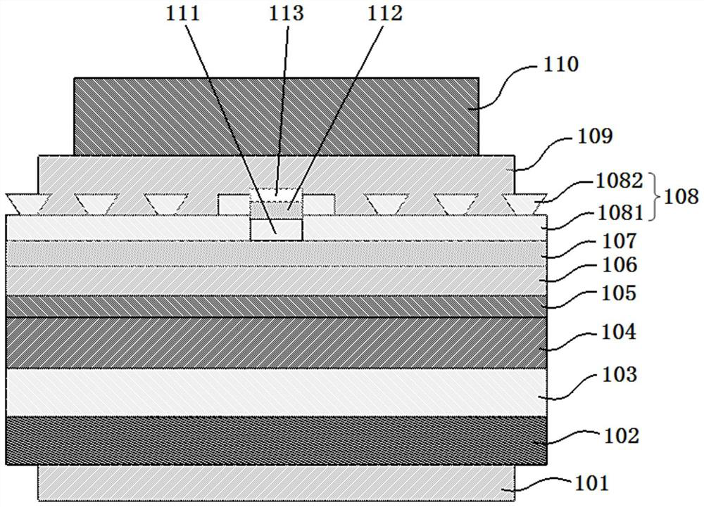
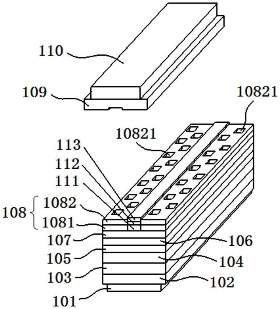
[0041] refer to figure 1 and figure 2 , a GaN-based laser diode structure according to an embodiment of the present invention includes an N electrode 101 , an n-type GaN substrate 102 , an N cladding layer 103 , an N waveguide layer 104 , a light-emitting active layer 105 , a P waveguide layer 106 , and an electron blocking layer 107 and passivation layer 108.

[0042] The n-type GaN substrate 102 ...


PUM


Abstract

The invention provides a GaN-based laser diode structure and a manufacturing method. The GaN-based laser diode structure comprises an N electrode, an n-type GaN substrate, an N covering layer, an N waveguide layer, a light-emitting active layer, a P waveguide layer, an electron blocking layer and a passivation layer which are sequentially arranged in a stacked mode. A ridge strip is arranged on the upper surface of the P-type electron barrier layer and comprises a P covering layer, and a P contact layer and a P contact electrode layer which are sequentially stacked on the P covering layer; the passivation layer comprises a first passivation layer and a second passivation layer which are arranged in a stacked mode, the first passivation layer is arranged on the upper surface of the P-type electron blocking layer and located on the two sides of the ridge strip, a groove is formed in the second passivation layer, a first metal layer is arranged on the upper surface of the second passivation layer and on the ridge strip, the first metal layer is provided with a protruding part corresponding to the groove, and a second metal layer is arranged on the protruding part. And a P electrode is arranged on the upper surface of the first metal layer. The stress of the electrode structure is reduced, the adhesive force between the metal electrode and the passivation layer is improved, a thick metal electrode can be formed, the packaging requirement is reduced, the heat dissipation performance is improved, and application is expanded.

Description

technical field [0001] The present invention relates to the technical field of GaN-based laser diodes, in particular to a GaN-based laser diode structure and a manufacturing method. Background technique [0002] For edge-emitting laser diodes, in order to form a good ridge waveguide structure, the side of the ridge is covered with an optical insulating layer of SiO 2 , can form an optical confinement, allowing the current to be injected from the ridge to form a high current density and reach the laser threshold; because the contact area of ​​the ridge is very small, the metal electrode and SiO 2 The adhesion of the high-power laser diode is poor, and the thick metal electrode has a large stress and is easy to fall off; therefore, the metal electrode of the high-power laser diode adopts a thin structure, which indirectly causes many problems in packaging, such as poor heat dissipation. SUMMARY OF THE INVENTION [0003] Based on this, the purpose of the present invention is...

Claims


Application Information

Patent Timeline
Patent Type & Authority Applications(China)
IPC IPC(8): H01S5/028H01S5/042H01S5/32H01S5/323
CPCH01S5/0282H01S5/3218H01S5/32341H01S5/04252H01S5/04254
Inventor 王程刚
Owner 安徽格恩半导体有限公司
Why Eureka
Try Eureka