Epitaxial structure and epitaxial growth method thereof, and LED chip

A technology of epitaxial growth and epitaxial structure, applied in the direction of sustainable manufacturing/processing, climate sustainability, semiconductor devices, etc., can solve problems such as insufficient brightness, and achieve the increase of saturation value of light intensity, increase of recombination efficiency, and increase of migration probability Effect

Pending Publication Date: 2022-06-03
JIANGXI ZHAO CHI SEMICON CO LTD
View PDF0 Cites 1 Cited by
  • Summary
  • Abstract
  • Description
  • Claims
  • Application Information

AI Technical Summary

Problems solved by technology

[0003] However, because the process of red and yellow GaAs LED front-mounted positive polarity chips is extremely simple at the chip manufacturing end, there is a defect of insufficient brightness. Currently, the brightness of 4mil to 5mil red-yellow GaAs LED front-mounted positive polarity chips with a relatively high market share is only 120mcd- Between 160mcd

Method used


Image

  • Epitaxial structure and epitaxial growth method thereof, and LED chip
  • Epitaxial structure and epitaxial growth method thereof, and LED chip

Examples


Embodiment 1

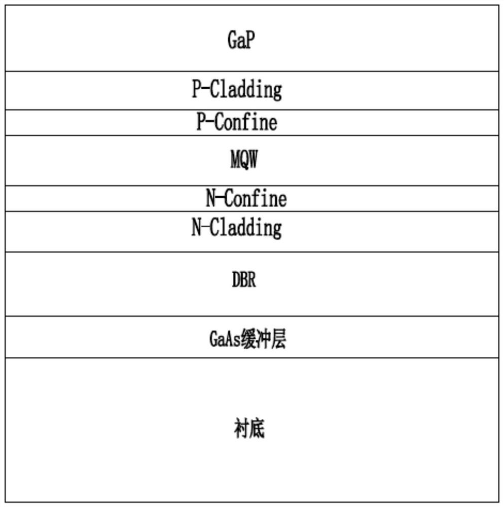
[0032] see figure 1 , shows the epitaxial structure in the first embodiment of the present invention, including a substrate, and a buffer layer, a Bragg reflector (Distributed Bragg Reflection, DBR for short), an N-type cladding layer (N-Cladding) epitaxially grown on the substrate in turn ), N-type confinement layer (N-Confine), multiple quantum well layer (Multiple Quantum Well, referred to as MQW), P-type confinement layer (P-Confine), P-type cladding layer (P-Cladding) and current spreading layer.

[0033] In some preferred cases of this embodiment, the substrate may be a GaAs substrate, the buffer layer may be a GaAs buffer layer, the Bragg mirror includes multiple pairs of alternately grown AlAs layers and GaAs layers, and the N-type cladding layer may be Si-doped AlInP layer, the multiple quantum well layer includes multiple pairs of alternately grown quantum well layers and quantum barrier layers, wherein the materials of the quantum well layer and the quantum barrier ...

Embodiment 2

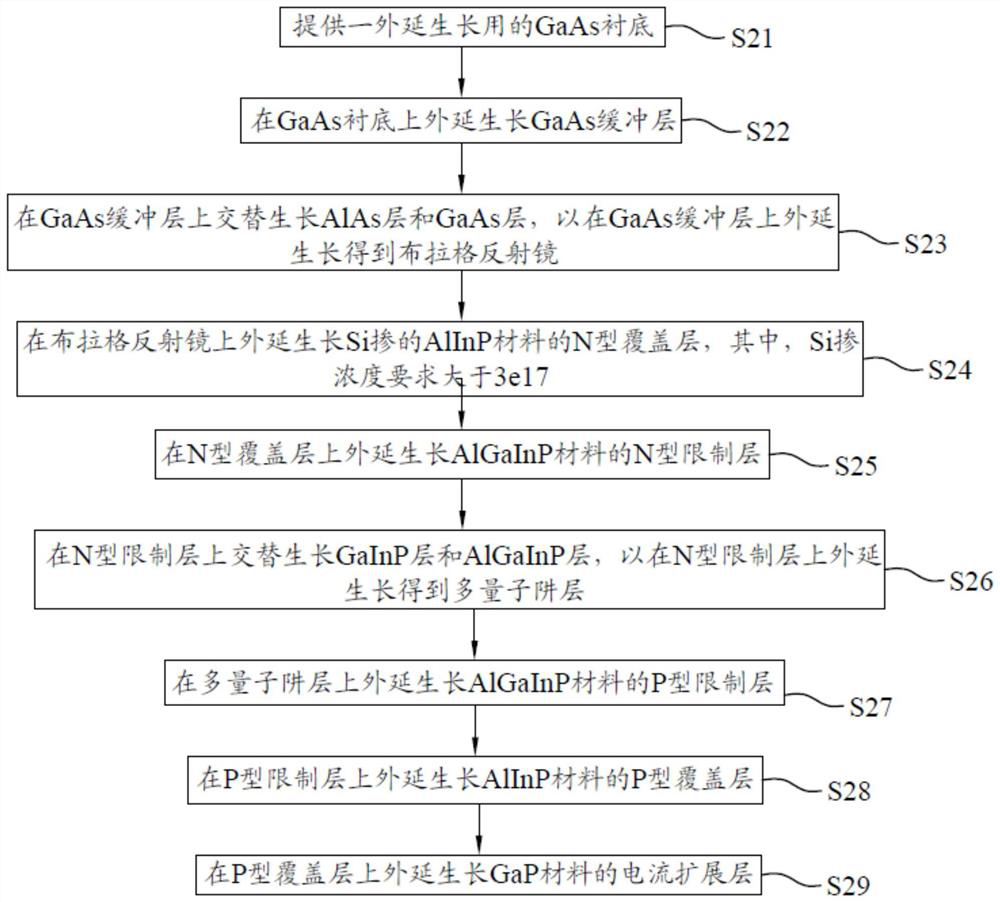
[0037] see figure 2 , shows an epitaxial growth method of an epitaxial structure proposed in the second embodiment of the present invention, which is used to prepare the epitaxial structure in the above-mentioned first embodiment. The method specifically includes steps S21 to S29, wherein:

[0038] Step S21, providing a GaAs substrate for epitaxial growth.

[0039] In step S22, a GaAs buffer layer is epitaxially grown on the GaAs substrate.

[0040] In step S23, AlAs layers and GaAs layers are alternately grown on the GaAs buffer layer to obtain a Bragg mirror by epitaxial growth on the GaAs buffer layer.

[0041] Step S24, epitaxially growing an N-type cladding layer of Si-doped AlInP material on the Bragg mirror, wherein the Si-doped concentration is required to be greater than 3e17 / cm 3 .

[0042] In step S25, an N-type confinement layer of AlGaInP material is epitaxially grown on the N-type cladding layer.

[0043] Step S26, alternately growing GaInP layers and AlGaIn...

Embodiment 3

[0049] The third embodiment of the present invention provides an LED chip, which includes the epitaxial structure in the first embodiment, and the epitaxial structure can be obtained by epitaxial growth by the epitaxial growth method of the epitaxial structure in the second embodiment.

[0050] To sum up, the epitaxial structure, the epitaxial growth method, and the LED chip in the embodiments of the present invention increase the N-layer carrier concentration by increasing the Si doping concentration of the N-type cladding layer, so that under the same conditions, the carrier migration The probability increases, which increases the recombination efficiency of the epitaxial PN junction. In addition, with the increase of the doping concentration of the N-type cladding layer, the logarithm of the barrier and the well is simultaneously increased in the multi-quantum well layer, which increases the limit of carrier overflow and increases the saturation value of the light intensity,...


PUM


Abstract

The invention provides an epitaxial structure and an epitaxial growth method thereof, and an LED chip, the epitaxial structure comprises a substrate, an N-type covering layer epitaxially grown on the substrate, and a multi-quantum well layer epitaxially grown on the N-type covering layer, and the multi-quantum well layer comprises a plurality of pairs of quantum well layers and quantum barrier layers which alternately grow; wherein the Si doping concentration of the N-type covering layer is greater than 3e17, and the logarithm of the quantum well layer and the quantum barrier layer is increased along with the increase of the Si doping concentration of the N-type covering layer. Besides, by increasing the Si doping concentration of the N-type covering layer, the carrier concentration of the N layer is improved, so that under the same condition, the carrier migration probability is increased, and the recombination efficiency of the epitaxial PN junction is improved. Besides, along with the increase of the doping concentration of the N-type covering layer, the number of pairs of barriers and wells of the multi-quantum well layer is increased synchronously, the limit of carrier overflow is improved, the light intensity saturation value is increased, and therefore the brightness of the chip can be higher under the same manufacturing process.

Description

technical field [0001] The invention relates to the technical field of LEDs, in particular to an epitaxial structure, an epitaxial growth method and an LED chip. Background technique [0002] Light Emitting Diode (LED) is a semiconductor electronic component that can emit light. Due to its small size, high brightness, and low energy consumption, it has attracted more and more researchers' attention. Among them, the red and yellow GaAsLED positive polarity chip is currently a very simple process, high market penetration rate and low price LED chip. [0003] However, because the red-yellow GaAs LED positive-polarity chip is extremely simple in the chip manufacturing process, it leads to the defect of insufficient brightness. At present, the 4mil-5mil red-yellow GaAs LED positive-polarity chip with a high market share has a brightness of only 120mcd- between 160mcd. SUMMARY OF THE INVENTION [0004] Based on this, the purpose of the present invention is to provide an epitax...

Claims


Application Information

Patent Timeline
Patent Type & Authority Applications(China)
IPC IPC(8): H01L33/06H01L33/00H01L33/10H01L33/12H01L33/14
CPCH01L33/0062H01L33/06H01L33/10H01L33/12H01L33/145Y02P70/50
Inventor 贾钊窦志珍兰晓雯杨琦胡加辉金从龙顾伟
Owner JIANGXI ZHAO CHI SEMICON CO LTD
Why Eureka
Try Eureka