Manufacturing method of MIM capacitor and MIM capacitor
A manufacturing method and capacitor technology, which are applied to capacitors, electro-solid devices, circuits, etc., can solve the problems of reduced capacitor performance, poor capacitor linearity performance, and reduced read-write and computing performance of mixing chips, so as to improve reliability. , the effect of reducing the temperature coefficient and improving the temperature linearity performance
- Summary
- Abstract
- Description
- Claims
- Application Information
AI Technical Summary
Problems solved by technology
Method used
Image

Examples
Embodiment 1
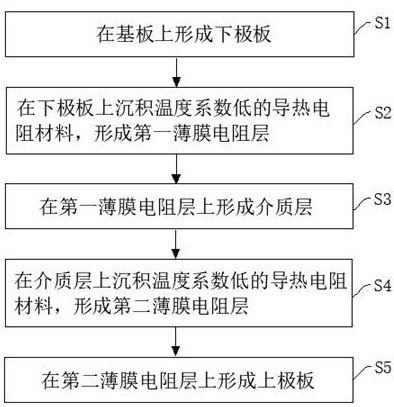
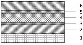
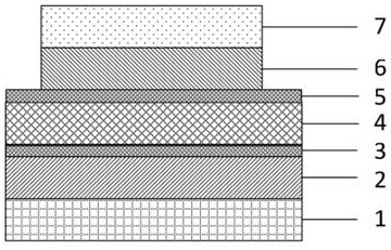
The method for manufacturing an MIM capacitor provided in this embodiment includes: a first step, refer to Figure 2A , deposit on the substrate 1 to form the lower electrode plate 2, deposit a thermally conductive resistance material with a low temperature coefficient on the lower electrode plate 2 to form the first thin film resistance layer 3; deposit on the first thin film resistance layer 3 to form a dielectric layer 4, on the dielectric layer 4, a thermally conductive resistance material with a low temperature coefficient is deposited on the second thin film resistance layer 5, so that the first thin film resistance layer 3 and the second thin film resistance layer 5 fully cover the dielectric layer 4; on the second thin film resistance layer 5, a conductive metal is deposited The material forms a material layer as the upper plate 6 . The second step, refer to Figure 2B , apply photoresist 7 on the material layer of the upper pole plate 6, form a photoresist pattern by ...
Embodiment 2
The method for manufacturing an MIM capacitor provided in this embodiment includes: a first step, refer to Figure 3A , deposit on the substrate 1 to form the lower electrode plate 2, deposit a thermally conductive resistance material with a low temperature coefficient on the lower electrode plate 2 to form the first thin film resistance layer 3; deposit on the first thin film resistance layer 3 to form a dielectric layer 4, on the dielectric layer 4, a thermally conductive resistance material with a low temperature coefficient is deposited on the second thin film resistance layer 5, so that the first thin film resistance layer 3 and the second thin film resistance layer 5 fully cover the dielectric layer 4; on the second thin film resistance layer 5, a conductive metal is deposited The material forms a material layer as the upper plate 6 . The second step, refer to Figure 3B , apply photoresist 7 on the material layer of the upper pole plate 6, form a photoresist pattern by ...
Embodiment 3
The method for manufacturing an MIM capacitor provided in this embodiment includes: a first step, refer to Figure 4A , deposit on the substrate 1 to form a lower electrode plate 2, deposit a thermally conductive resistance material with a low temperature coefficient on the lower electrode plate 2 to form a first thin film resistance layer 3; deposit on the first thin film resistance layer 3 to form a dielectric layer 4, on the dielectric layer A second thin film resistance layer 5 is formed by depositing a thermally conductive resistance material with a low temperature coefficient on 4, and the first thin film resistance layer 3 and the second thin film resistance layer 5 fully cover the dielectric layer 4; on the second thin film resistance layer 5, a conductive metal is deposited The material forms a material layer as the upper plate 6 . The second step, refer to Figure 4B , apply photoresist 7 on the material layer of the upper pole plate 6, form a photoresist pattern by ...
PUM
| Property | Measurement | Unit |
|---|---|---|
| Temperature coefficient | aaaaa | aaaaa |
| Thickness | aaaaa | aaaaa |
Abstract
Description
Claims
Application Information