Device and method for eliminating optical fiber end face reflected light noise and manufacturing method
An optical fiber end face, reflected light technology, applied in the field of sensing, can solve the problems of knotting and smearing of the tail end, difficult to maintain for a long time, lack of space, etc., to reduce the noise of reflected light and improve the measurement accuracy.
- Summary
- Abstract
- Description
- Claims
- Application Information
AI Technical Summary
Problems solved by technology
Method used
Image
Examples
Embodiment 1
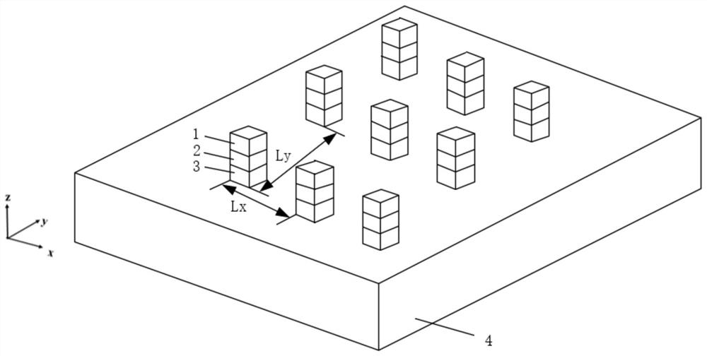
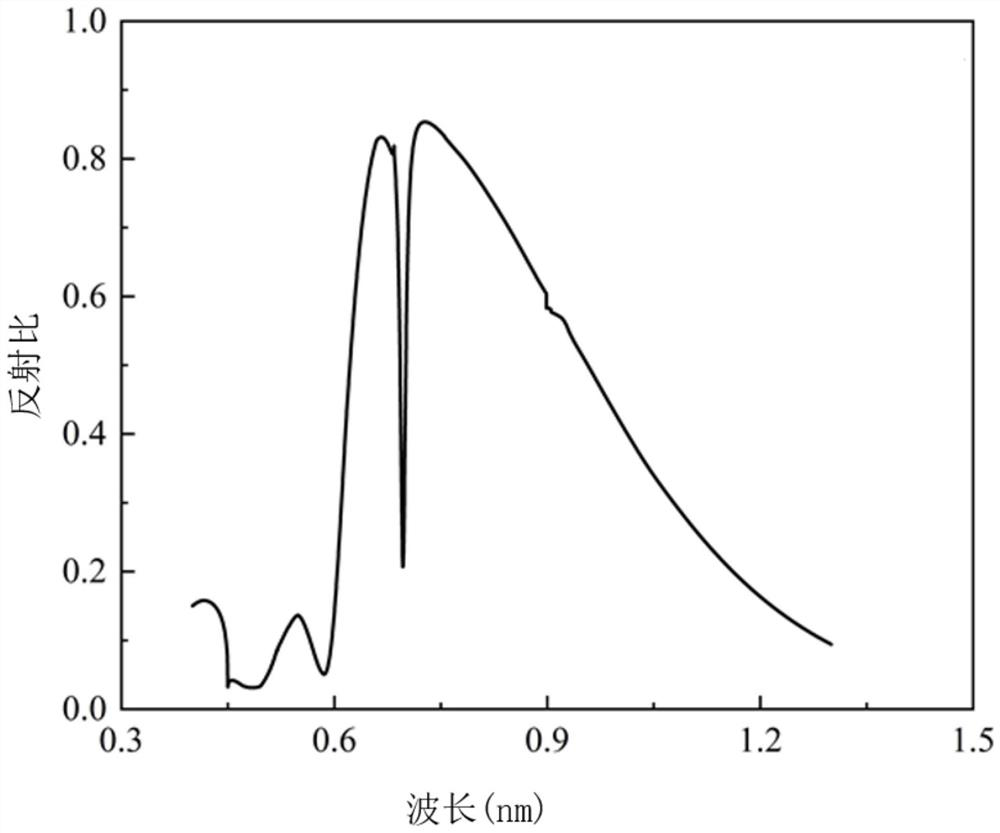
[0062] This embodiment provides a device, method and manufacturing method for eliminating the reflected light noise from the end face of an optical fiber:
[0063] Specifically, the refractive index of silicon dioxide 2 is 1.41, the refractive index of air is 1.0, the thickness of silicon substrate 4 is 400 nm, the refractive index of silicon substrate 4 is 1.43, the side length of square nano-columns is 160 nm, and the silicon dioxide 2 The thickness of 130nm, the nanopillar spacing in the y direction is 450nm, the spacing in the x direction is 200nm, the thickness of the first metal ridge 1 is 130nm, and the thickness of the second metal ridge 3 is 130nm.
Embodiment 2
[0065] This embodiment provides a device, method and manufacturing method for eliminating the reflected light noise from the end face of an optical fiber:
[0066] Specifically, the refractive index of silicon dioxide 2 is 1.49, the refractive index of air is 1.0, the thickness of silicon substrate 4 is 600 nm, the refractive index of silicon substrate 4 is 1.55, the side length of square nano-columns is 200 nm, and the silicon dioxide 2 The thickness of 180nm, the nanopillar spacing in the y direction is 200nm, the spacing in the x direction is 450nm, the thickness of the first metal ridge 1 is 180nm, and the thickness of the second metal ridge 3 is 180nm.
Embodiment 3
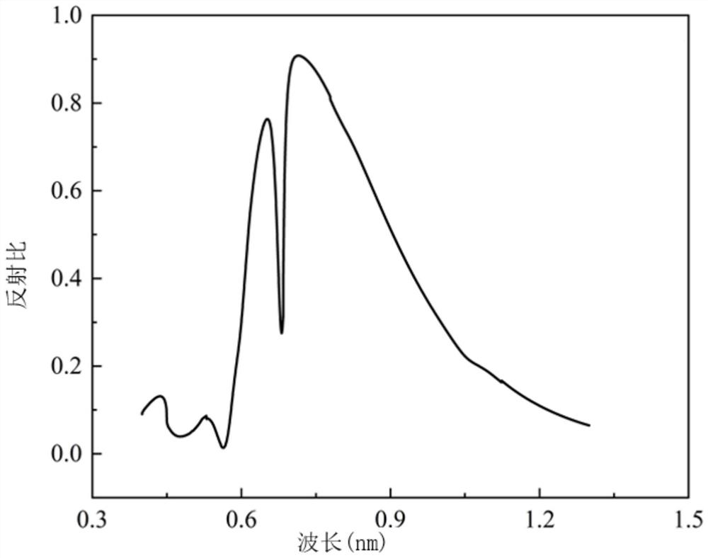
[0068] This embodiment provides a device, method and manufacturing method for eliminating reflected light noise from the end face of an optical fiber, such as figure 2 As shown, compared with Embodiment 1, the main difference of this embodiment is:
[0069] Specifically, the refractive index of the silicon dioxide 2 is 1.45, the refractive index of air is 1.0, the thickness of the silicon substrate 4 is 500 nm, the refractive index of the silicon substrate 4 is 1.52, the side length of the square nano-column is 180 nm, and the silicon dioxide 2 The thickness of the nano-pillars is 160 nm, the spacing of the nano-pillars in the y-direction is 450 nm, the spacing in the x-direction is 400 nm, the thickness of the first metal ridge 1 is 140 nm, and the thickness of the second metal ridge 3 is 140 nm. Reflection spectrum, the peak value is 681 nm , the reflection intensity is 27%.
PUM
| Property | Measurement | Unit |
|---|---|---|
| thickness | aaaaa | aaaaa |
| width | aaaaa | aaaaa |
| thickness | aaaaa | aaaaa |
Abstract
Description
Claims
Application Information


