Quantitative detection method for glare defect of optical lens
A quantitative detection method and optical lens technology, applied in the field of optics, can solve problems such as poor accuracy, poor consistency and repeatability, inconvenient and intuitive viewing of test results, failure to meet quality and efficiency requirements, etc., and achieve uniform and neat distribution of light spots , easy to view directly, and high production efficiency
- Summary
- Abstract
- Description
- Claims
- Application Information
AI Technical Summary
Problems solved by technology
Method used
Image
Examples
Embodiment 1
[0035] like figure 1 As shown in the figure, a quantitative detection method for glare defects of an optical lens includes the following steps:
[0036] Sp1: Assembly of equipment: installation of test target and tested target;
[0037] Sp2: image acquisition: the setting of the value, the image acquisition of the tested target and transmission to the computer 4 for saving;
[0038] Sp3: Image processing: process the original image through luminance binarization;
[0039] Sp4: Image classification: The spot image and background image of the extracted and processed image are classified and saved;
[0040] Sp5: Analysis of spot image: analyze the image of the classified spot image and compare it with the standard sample;
[0041] Sp6: Background image analysis: image analysis of the classified background image;
[0042] Sp7: Analysis of multiple binarization thresholds: Set multiple different binarization parameters to analyze the image.
Embodiment 2
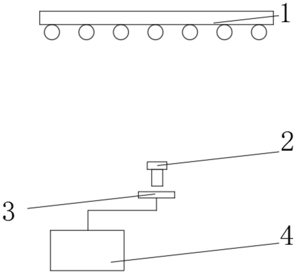
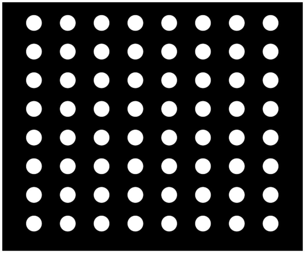
[0044] like Figure 2-4 As shown in the figure, the circular light source array 1 with a black background is the detection target, and the target light board is a light-emitting array composed of 64 to 100 light-emitting diodes equally spaced and evenly distributed. 4500K-6500K, the luminous flux is more than 200 lumens, the background of the lamp board is blackened, the video sensor chip 3 matches the imaging area and imaging resolution of the tested lens 2, the video sensor chip 3 is a picture acquisition device, and the circular light source array 1 is located in The top surface of the lens under test 2, the bottom of the lens under test 2 is placed with a video sensor chip 3, the video sensor chip 3 is electrically connected to the computer 4, and the position where the lens under test 2, the video sensor chip 3 and the circular light source array 1 are installed is in the imaging position The proper position of the optical axis makes the image clear, the field of view is ...
Embodiment 3
[0046] like Figure 5-9As shown in the figure, the threshold parameter of binarization is set by the user, and the binarization processes the image saved by the computer 4. After the binarization image is processed, the bright part is the spot image, and the remaining part of the bright part is the background image, and the spot is analyzed. The quality of each circular spot is shown in the figure. The quality analysis includes the area of each circular spot and the circularity of the single-point spot, which can display a single ring in a bad area. The quality distribution of the single point in the The point mass distribution is compared with the single point mass distribution of the standard sample, and the quality of the spot image of the tested lens 2 is graded. The video sensor chip 3 is electrically connected to the computer 4, and the image is collected and transmitted to the computer 4 for storage. The user can set two values. The brightness binarization process is ...
PUM
 Abstract
Description
Claims
Application Information


