Artificial surface plasmon polariton and microstrip line conversion structure and method

A plasma and artificial surface technology, applied in the field of plasma, can solve the problems of large size, increase the difficulty of processing, difficult to achieve effects, etc., and achieve the effects of low processing difficulty, miniaturization and compact structure

Active Publication Date: 2022-06-24
BEIJING UNIV OF POSTS & TELECOMM +1
3 Cites 0 Cited by

AI-Extracted Technical Summary

Problems solved by technology

However, this conversion structure needs to add an additional metal strip structure along the groove direction, which is not conducive to processing and integrating other devices in this direction, and the size of the period is at least larger than 1 SSPPs
In addition, the conversion structure is applied in the microwave frequency band. If it is applied in the millimeter wave and terahertz frequency bands, the...

Method used

Because the phase shift constant of the artificial surface plasmon is higher than the phase shift constant of the microstrip line, the stepped structure of the metal patch will increase the phase shift constant of the electromagnetic wave from the microstrip line as the step width increases , or the phase shift constant of the electromagnetic wave from the artificial surface plasmon decreases with the step width decreasing, and the transition microstrip line plays a role of transition, so that the microstrip line and the artificial surface plasmon in the electromagnetic wave transmission mode Transformation is more adaptable.
[0049] In Fig. 1, ② the conversion structure includes three steps, which are the key components for the realization of the conversion. Fig. 3 is a schematic diagram of the structure of the ladder-shaped metal sheet of the conversion structure in an embodiment of the present invention. Disassemble the structur...

Abstract

The invention provides an artificial surface plasmon polariton and microstrip line conversion structure and method, the conversion structure comprises a metal patch and a transition microstrip line, the metal patch is a step-shaped structure with gradually increased width, and the width of the metal patch is the size of the metal patch perpendicular to the electromagnetic wave propagation direction; the side, with the smaller width, of the metal patch is connected with the microstrip line, and the side, with the larger width, of the metal patch is connected with the transition microstrip line. One side of the transition microstrip line is connected with the metal patch, and the other side of the transition microstrip line is connected with the artificial surface plasmon polaritons. Mode matching and conversion between the microstrip line and SSPPs can be achieved, no extra metal patch needs to be introduced, integration between different devices is facilitated, the machining difficulty is low, the structure is compact, the size is small, and miniaturization of the devices can be achieved. When the antenna is applied to millimeter wave and terahertz frequency bands, the loss is small and the processing difficulty is low.

Application Domain

WaveguidesCoupling devices

Technology Topic

Frequency bandPolariton +8

Image

  • Artificial surface plasmon polariton and microstrip line conversion structure and method
  • Artificial surface plasmon polariton and microstrip line conversion structure and method
  • Artificial surface plasmon polariton and microstrip line conversion structure and method

Examples

  • Experimental program(1)

Example Embodiment

[0032] In order to make the objectives, technical solutions and advantages of the present invention clearer, the present invention will be further described in detail below with reference to the embodiments and accompanying drawings. Here, the exemplary embodiments of the present invention and their descriptions are used to explain the present invention, but not to limit the present invention.
[0033] Here, it should also be noted that, in order to avoid obscuring the present invention due to unnecessary details, only the structures and/or processing steps closely related to the solution according to the present invention are shown in the drawings, and the related structures and/or processing steps are omitted. Other details not relevant to the invention.
[0034] It should be emphasized that the term "comprising/comprising" when used herein refers to the presence of a feature, element, step or component, but does not exclude the presence or addition of one or more other features, elements, steps or components.
[0035] Here, it should also be noted that, if there is no special description, the term "connection" herein may not only refer to direct connection, but also to indicate indirect connection with intermediates.
[0036] Hereinafter, embodiments of the present invention will be described with reference to the accompanying drawings. In the drawings, the same reference numbers represent the same or similar parts, or the same or similar steps.
[0037] In order to solve the problems of large size, low device integration and difficult application in the millimeter wave and terahertz frequency bands of the existing artificial surface plasmon polariton and microstrip line conversion structure, the present invention provides an artificial surface. Plasmon-to-microstrip switching structures and methods.
[0038] In the artificial surface plasmon and microstrip line conversion structure of the present invention, the conversion structure includes a metal patch and a transition microstrip line, the metal patch is a stepped structure with increasing width, and the width of the metal patch is perpendicular to the propagation of electromagnetic waves. The size of the metal patch in the direction of One side of the wire is connected to the metal patch, and the other side is connected to the artificial surface plasmon.
[0039] Based on the stepped metal patch, the conversion between SSPPs and microstrip lines is realized. The stepped metal patch has a small width in the propagation direction of electromagnetic waves, which can realize miniaturization, and can match the wave vector of SSPPs and microstrip lines, so as to realize the conversion of SSPPs and microstrip lines. This conversion structure can be applied to the conversion of SSPPs and microstrip lines in the millimeter wave and terahertz frequency bands, with low loss and low processing difficulty.
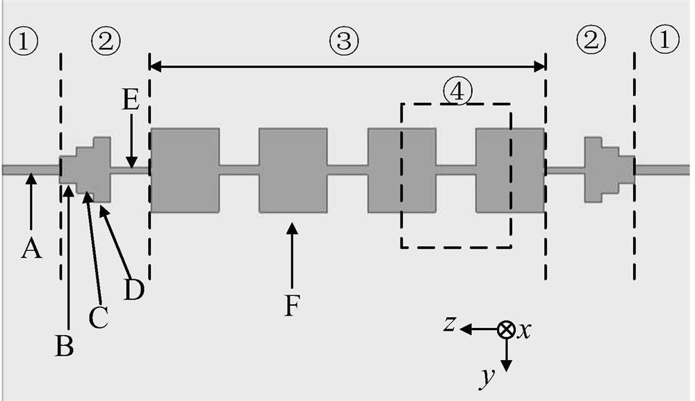
[0040] figure 1 It is a plan view of a back-to-back overall structure of SSPPs and microstrip line conversion in an embodiment of the present invention. Area ① in the figure is the microstrip line feeder, ② is the conversion structure of the present invention, including metal patches and transition microstrip lines, ③ is the SSPPs part, and ④ is an SSPPs unit. The six positions marked A, B, C, D, E, and F are the cross sections of the microstrip line, step 1, step 2, step 3, transition microstrip line and SSPPs on the xy plane, respectively. The x-y-z axis can better express the position, size and propagation direction of electromagnetic waves. In the embodiment of the present invention, the overall structure is symmetrical about the center line of ③, but this symmetry is not necessary. The purpose is to demonstrate that in practical applications, the microstrip line is converted to SSPPs, transmitted on SSPPs for a period of time, and then The actual use process of converting to microstrip line.
[0041] In the embodiment of the present invention, the material of the metal patch is gold, and the thickness is 1 μm. This embodiment is a preferred embodiment, and the material and thickness of the metal patch can be adjusted according to the actual situation. For example, the material of the metal patch is copper, and the thickness is 2 μm. In actual design, it can be optimized according to needs, through adjustment and testing Find the optimal solution.
[0042] In the embodiment of the present invention, the metal patch is a three-layer stair-like structure of equal length. The length of each step of the metal patch refers to the size of the metal patch along the electromagnetic wave propagation direction, and the width of each step of the metal patch refers to the size of the metal patch perpendicular to the electromagnetic wave propagation direction. The embodiment of the present invention is a preferred embodiment , the number of steps and the actual width of the metal patch can be adjusted according to the actual situation, such as changing to 4 steps, and the length of the steps can be adjusted.
[0043] In the embodiment of the present invention, the metal patch is attached to the front side of the dielectric plate, the dielectric is high-resistance silicon, the relative permittivity is 11.62, the loss tangent is 10-4, and the thickness is 23 μm. figure 1 The front structure of the dielectric board is shown, and the back of the dielectric board is covered by a layer of metal ground with a thickness of 1 μm and the material is gold. This embodiment is a preferred embodiment, and the dielectric plate can be adjusted to other materials and sizes, and adjusted according to the actual situation.
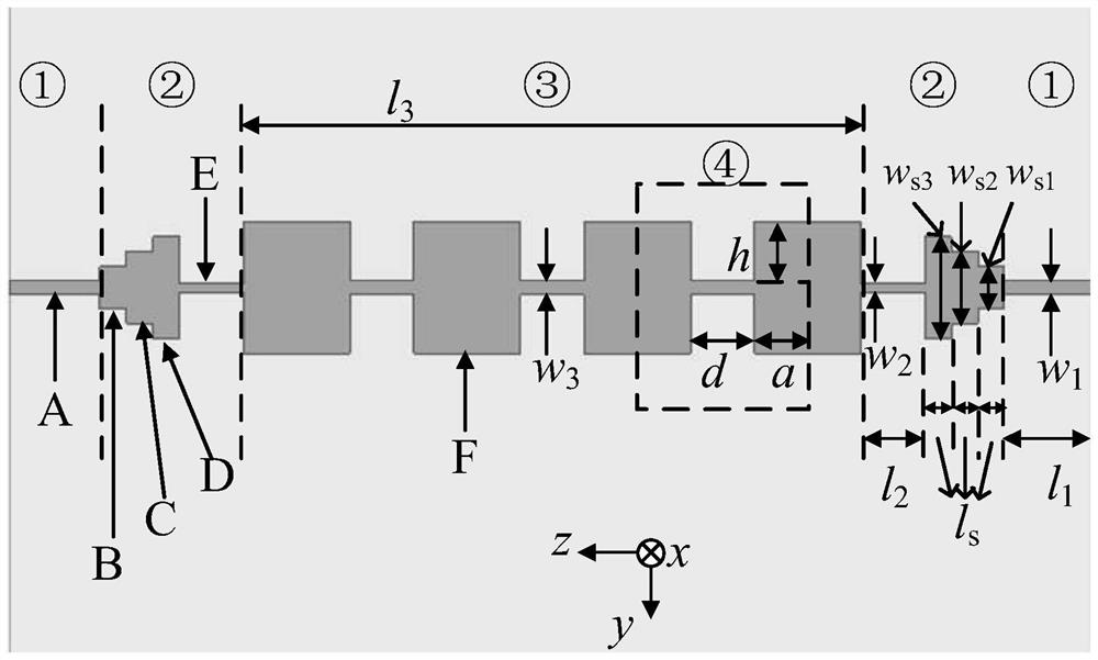
[0044] figure 2 It is a back-to-back overall structure and size plan of the SSPPs and microstrip line conversion in an embodiment of the present invention, and the structure is the same as figure 1 The same, but the dimensions of each structure are marked in detail. Among them: ① is the microstrip line feeder, the width is w 1 , the length is l 1. ②Consists of a stepped metal patch and a section of microstrip line. The metal patch consists of three steps, the widths of steps 1, 2, and 3 are respectively w s1 , w s2 , w s3 , the length is l s. The transition microstrip line width is w 2 , the length is l 2. ③ is a transmission line composed of SSPPs, with a total length of l 3. ④ is an H-type SSPPs unit, the size is from a, d, h, w 3 Determined, the length of one unit period is d+a*2, and the width of the central strip line is w 3 set to the width w of the microstrip feeder 1 the same, so no additional impedance matching structures are required. figure 2 The specific dimensions of the structures are summarized in Table 1.
[0045] Table 1 figure 1 The specific size of the overall structure in the middle (unit: μm)
[0046]
[0047] It should be noted that the above dimensions are only used as preferred embodiments and do not limit the dimensions of the present invention. In the actual production process, adaptive adjustments can be made according to different structures of microstrip lines and artificial surface plasmons.
[0048] In this embodiment of the present invention, the artificial surface plasmon includes a plurality of artificial surface plasmon units, wherein the width of the center stripline of the artificial surface plasmon unit is the same as the width of the microstrip line feeder, so No additional impedance matching structures are required.
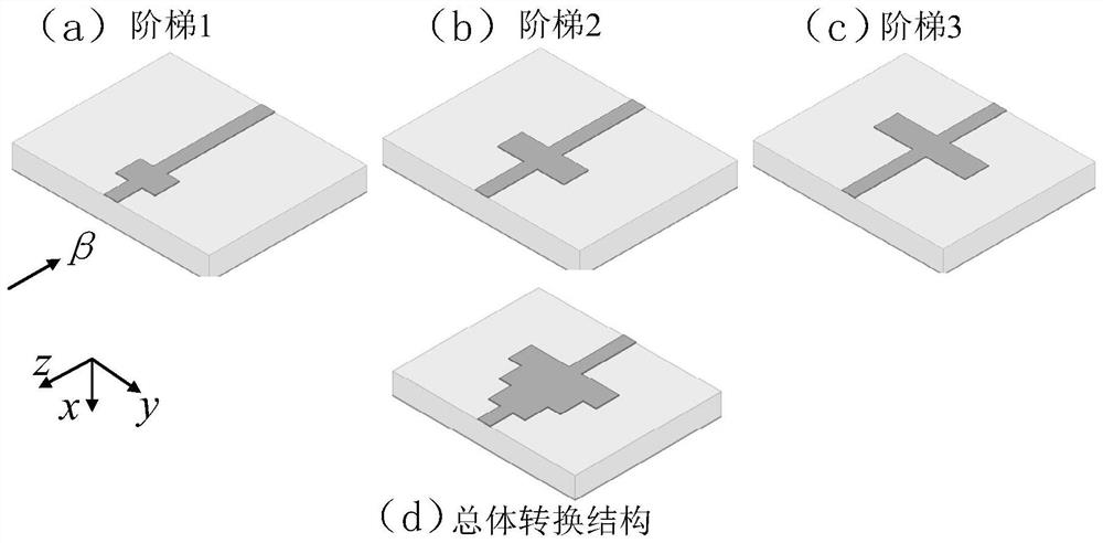
[0049] figure 1 Medium ② The conversion structure contains three steps, which are the key components of the conversion implementation. image 3 It is a schematic diagram of the stepped metal sheet structure of the conversion structure in an embodiment of the present invention. Will figure 1 The structure ② in is disassembled into (a) step 1; (b) step 2; (c) step 3; (d) overall conversion structure. Figure 4 A schematic diagram of the structure of the SSPPs unit in an embodiment of the present invention, such as Figure 4 As shown, several unit periods are set to the period d+a*2 (160 μm) of SSPPs, and the electromagnetic wave is along the opposite direction of the z-axis (that is, β is along the -z direction, and the same is true when β is along the +z direction). Preferably, the length of the switching structure in the embodiment of the present invention is 135 μm, the length of the SSPPs unit period is 160 μm, and the length of the switching structure is only 0.84 unit period of the SSPPs. The stepped SSPPs and the microstrip line conversion structure proposed by the present invention have a compact structure, shorten the length of the conversion structure, and can achieve lower losses in the millimeter wave and terahertz frequency bands.
[0050] The working principle of this conversion structure is described below from the perspective of the dispersion curve. The HFSS eigenmode is used to solve the problem, and the dispersion curves of the SSPPs cell, microstrip line, step 1, step 2, step 3, and overall conversion structure are plotted in Figure 5 middle. like Figure 5 As shown, at the same frequency, the phase shift constant of the microstrip line is smaller than that of SSPPs (the phase shift constant is used to characterize the phase shift value of the electromagnetic wave when it is transmitted along a uniform line of unit length), so the mode does not match between the two. Steps 1, 2, and 3 gradually increase the phase shift constant of the microstrip line, and finally the phase shift constant of the overall conversion structure is close to that of step 3. The step-shaped conversion structure can increase the phase shift constant of the microstrip line. At the same time, since the phase shift constant is not abrupt, but gradually changes through the steps, the matching between the microstrip line and the SSPPs can be realized. In addition, the width of the access after optimizing the ladder is w 2 , the length is l 2 The transition microstrip line can further improve the matching effect of the transition structure and SSPPs. The width and length of steps 1, 2, and 3 can be optimized according to different SSPPs structures, and the values ​​given in Table 1 are only examples.
[0051] Depend on Figure 5 It can be seen from the displayed dispersion curve that in the process from the microstrip line to step 1, step 2, step 3, and transition microstrip line (as can be seen from the dispersion curve passing through the overall conversion structure), the electromagnetic wave is reversed along the z-axis. direction transmission, the dispersion curve is more and more close to the dispersion curve of SSPPs.
[0052] The working principle of this conversion structure will be described below from the perspective of electric field distribution. Image 6 It is a vector distribution diagram of electric field intensity at different positions at 170 GHz in an embodiment of the present invention. Among them, the five positions A, B, C, D, and F are the microstrip line, step 1, step 2, step 3, and the cross-section of SSPPs on the xy plane. area, black is the area with smaller electric field intensity. In HFSS, the electric field intensity vector distribution of these five positions at 170 GHz can be obtained, and the electric field intensity adopts a uniform scale, such as Image 6 shown. Among them, the microstrip line at section A propagates the quasi-TEM mode, and the electric field is mainly concentrated near the metal strip; while at section F, the electric field in SSPPs is concentrated at the two edges in the y direction. At the step, that is, in the process of B→C→D, the electric field gradually approaches the electric field distribution of SSPPs from the microstrip line, so the mode conversion can be realized.
[0053] In the embodiment of the present invention, due to the dispersion curve characteristics of SSPPs, the overall structure has low-pass filtering characteristics. To verify this characteristic, S-parameters (Scatter, scattering parameters) are used to describe the frequency domain characteristics of the transmission channel. Figure 7 is the S-parameter of the back-to-back overall structure of the SSPPs and microstrip line conversion in an embodiment of the present invention. Among them, the bandwidth of S11
[0054] In some embodiments of the present invention, each step of the stepped structure of the metal patch is a rectangular structure or a trapezoidal structure, such as Figure 8 and Figure 10 shown.
[0055] In some embodiments of the present invention, the stepped structure of the metal patch in the conversion structure includes at least two layers of steps.
[0056] In this embodiment of the present invention, as figure 1 and figure 2 As shown, the metal patch in the conversion structure is a three-layer stepped structure of equal length.
[0057] In some embodiments of the present invention, the number of steps is not necessarily 3, and 3 steps are selected here to minimize the length of the conversion section under the condition of matching, so as to make the structure more compact. And each step of the metal patch is not necessarily the same length, and can be designed according to the actual situation.
[0058] In some embodiments of the present invention, the structure of the metal patch may be hollow, such as Figure 8 shown, Figure 9 for Figure 8 The S-parameter of the conversion structure, S11
[0059] Another aspect of the present invention provides a conversion method based on any one of the above-mentioned artificial surface plasmon polaritons and microstrip line conversion structures, characterized in that: when electromagnetic waves propagate from the microstrip line to the artificial surface plasmon polaritons , the metal patch receives the electromagnetic wave from the microstrip line, and then propagates to the transition microstrip line, and the transition microstrip line propagates the electromagnetic wave to the artificial surface plasmon; when the electromagnetic wave propagates from the artificial surface plasmon to the Microstrip line, the transition microstrip line receives electromagnetic waves from artificial surface plasmons and propagates to the metal patch, which propagates the electromagnetic waves to the microstrip line.
[0060]Because the phase shift constant of the artificial surface plasmon is higher than that of the microstrip line, the stepped structure of the metal patch will increase the phase shift constant of the electromagnetic wave from the microstrip line as the step width increases, or will The phase shift constant of the electromagnetic wave from the artificial surface plasmon decreases as the step width decreases, and the transition microstrip line plays the role of transition, making the microstrip line and the artificial surface plasmon more efficient in the transition of the electromagnetic wave transmission mode. adaptation.
[0061] In an embodiment of the present invention, when the electromagnetic wave propagates in the reverse direction of the z-axis, the left side of ① is port 1. After the energy is fed into the microstrip line, it enters the conversion structure of ②, and passes through the stepped metal patch and a section of the microstrip line. Then convert to SSPPs mode, then enter ③, then enter the conversion structure of ②, after a section of microstrip line and stepped metal patch, convert to microstrip line mode, and finally enter ①, output from port 2 on the right. Electromagnetic waves propagate in the positive z direction in exactly the same way as described above. combine image 3 It can be seen that the phase shift constant of the cell increases correspondingly when the step height increases. The conversion structure needs to match the microstrip line to the SSPPs with a higher phase shift constant, so the phase shift constant needs to be continuously increased in the matching structure, that is, the step heights increase sequentially. The size and scale of the transition structure ② can be optimized according to the simulation. When the electromagnetic wave propagates along the z-axis, it is converted from SSPPs to microstrip lines in the same way.
[0062] It is to be understood that the present invention is not limited to the specific arrangements and processes described above and shown in the figures. For the sake of brevity, detailed descriptions of known methods are omitted here. In the above-described embodiments, several specific steps are described and shown as examples. However, the method process of the present invention is not limited to the specific steps described and shown, and those skilled in the art can make various changes, modifications and additions, or change the sequence of steps after comprehending the spirit of the present invention.
[0063] In the present invention, features described and/or illustrated with respect to one embodiment may be used in the same or similar manner in one or more other embodiments, and/or in combination with or in place of features of other embodiments Features of the implementation.
[0064] The above descriptions are only preferred embodiments of the present invention, and are not intended to limit the present invention. For those skilled in the art, various modifications and changes may be made to the embodiments of the present invention. Any modification, equivalent replacement, improvement, etc. made within the spirit and principle of the present invention shall be included within the protection scope of the present invention.

PUM

PropertyMeasurementUnit
Thickness1.0µm

Description & Claims & Application Information

We can also present the details of the Description, Claims and Application information to help users get a comprehensive understanding of the technical details of the patent, such as background art, summary of invention, brief description of drawings, description of embodiments, and other original content. On the other hand, users can also determine the specific scope of protection of the technology through the list of claims; as well as understand the changes in the life cycle of the technology with the presentation of the patent timeline. Login to view more.

Similar technology patents

Preparation method of CaCu3Ti4O12 ceramic

Owner:NORTHWESTERN POLYTECHNICAL UNIV

Connector locking and electromagnetic unlocking device

ActiveCN101908691Acompact structurereliable unlock
Owner:GUIZHOU SPACE APPLIANCE CO LTD

Classification and recommendation of technical efficacy words

  • small size
  • compact structure

Microfabricated elastomeric valve and pump systems

InactiveUS6929030B2high speedsmall size
Owner:CALIFORNIA INST OF TECH

RFID antenna

InactiveUS20060208900A1high efficiencysmall size
Owner:TRANSPACIFIC TECH

Capacitor module, power converter, vehicle-mounted electrical-mechanical system

ActiveUS20070109715A1reduce surge voltagesmall size
Owner:HITACHI ASTEMO LTD

Projection display chip

InactiveUS20100321640A1small sizehigh efficiency
Owner:IND TECH RES INST

Phase-change energy-storage material nanocapsule and preparation method thereof

ActiveCN104449590Asmall sizeImprove stability
Owner:INST OF CHEM MATERIAL CHINA ACADEMY OF ENG PHYSICS

Smart home system based on internet of things cloud computing

Owner:中国联合网络通信有限公司物联网研究院

Bionic underwater chelonian robot

InactiveCN101134500ACloselycompact structure
Owner:HARBIN ENG UNIV
Why Eureka
Try Eureka