Manufacturing method of array substrate, display panel and display device

A technology of an array substrate and a manufacturing method, applied in the display field, can solve the problems of not being too long in etching time, reducing the contact area, reducing the yield rate, etc., and achieving the effects of reducing the risk of explosion, ensuring the contact area, and reducing the risk of explosion.

Pending Publication Date: 2022-06-28
HKC CORP LTD
View PDF0 Cites 0 Cited by
  • Summary
  • Abstract
  • Description
  • Claims
  • Application Information

AI Technical Summary

Problems solved by technology

One of the ways to reduce the yield is to improve the opening defect of the protective layer (PV hole defect, Passivation hole defect). The general PV hole defect is mainly a fracture under the protective layer (PV undercut, Passivation undercut), which refers to the formation of PV holes. The rupture of the protective layer will cause abnormalities in the film formation of the subsequent indium tin oxide liner (ITO), which will eventually lead to ITO damage
[0003] The reason for the breakage of the protective layer is that after the protective layer is coated and exposed, it is developed and etched. The etching time should not be too long (other problems will occur when etching for a long time), so that the protective layer will remain in the hole and cover a part of the PV hole, resulting in PV. The hole becomes smaller, or the protective layer will form an irregular layer inside the PV hole, affecting the pore size of the PV hole
After the ITO coating is completed, the power is turned on. Since the PV hole diameter becomes smaller, the contact area between the corresponding ITO and the metal layer becomes smaller, and the resistance value may be too large, which may cause a risk of explosion.

Method used


Image

  • Manufacturing method of array substrate, display panel and display device
  • Manufacturing method of array substrate, display panel and display device
  • Manufacturing method of array substrate, display panel and display device

Examples


Embodiment 1

[0047] The present application provides a method for fabricating the array substrate 100 .

[0048] Please refer to figure 1 , Figure 4 and Figure 5 , in an embodiment of the present application, the manufacturing method of the array substrate 100 proposed in the present application includes the steps:

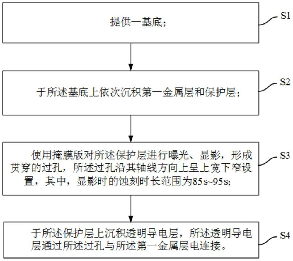
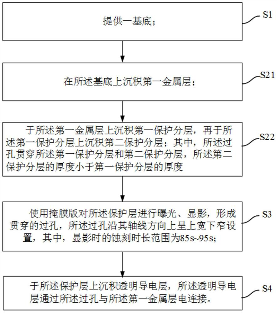
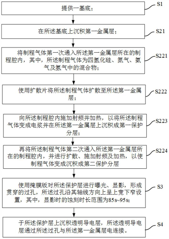
[0049] Step S1: providing a substrate 10;

[0050] Step S2: depositing a first metal layer 20 and a protective layer 30 on the substrate 10 in sequence;

[0051] Step S3 : using a mask to expose and develop the protective layer 30 to form a through hole 31 , and the via hole 31 is arranged in an upper width and a lower width along the axis direction, wherein the etching duration during development ranges 85s~95s;

[0052] Step S4 : depositing a transparent conductive layer 40 on the protective layer 30 , and the transparent conductive layer 40 is electrically connected to the first metal layer 20 through the via hole 31 .

[0053] It can be understood that the array subs...

Embodiment 2

[0085] Please refer to Figure 9 , the present application also proposes a display panel, the display panel includes an array substrate 100, a color filter substrate 700, and a liquid crystal layer 800 sandwiched between the array substrate 100 and the color filter substrate, the array substrate 100 adopts It is prepared as in the method for fabricating the array substrate 100 in any of the above embodiments. Since the present display panel adopts all the technical solutions of the above-mentioned embodiments, it has at least all the beneficial effects brought by the technical solutions of the above-mentioned embodiments, which will not be repeated here.

[0086] In this embodiment, the display panel may be a liquid crystal display panel, a self-luminous display panel, or the like, which is not limited herein. As an example, the display panel is a liquid crystal display panel, which includes an array substrate 100 and a color filter substrate 700 that are attached to each oth...

Embodiment 3

[0089] Please refer to Figure 10 , the present application also proposes a display device, the display device includes a backlight module 900 and a display panel arranged opposite to the backlight module 900, the display panel is the display panel described in any of the above embodiments. Since the display panel in the present display device adopts all the technical solutions of all the above-mentioned embodiments, it has at least all the beneficial effects brought by the technical solutions of the above-mentioned embodiments, which will not be repeated here.


PUM


Abstract

The invention discloses a manufacturing method of an array substrate, a display panel and a display device.The manufacturing method of the array substrate comprises the steps that a substrate is provided; sequentially depositing a first metal layer and a protective layer on the substrate; a mask is used for exposing and developing the protective layer, a through via hole is formed, the via hole is arranged in the mode that the upper portion is wide and the lower portion is narrow in the axis direction of the via hole, and the etching duration during developing ranges from 85 s to 95 s; and depositing a transparent conductive layer on the protective layer, wherein the transparent conductive layer is electrically connected with the first metal layer through the via hole. According to the technical scheme, the fracture risk of the via hole of the protection layer can be reduced, the aperture and gradient size of the via hole are ensured, and the product yield is improved.

Description

technical field [0001] The present application relates to the field of display technology, and in particular, to a manufacturing method of an array substrate, a display panel and a display device. Background technique [0002] With the continuous development of display technology, the improvement of product yield has also received more attention. One of the ways to reduce the yield is to improve the opening defect of the protective layer (PV hole defect, Passivation hole defect). The general PV hole defect is mainly the fracture under the protective layer (PV undercut, Passivation undercut), which refers to the formation of PV holes. When the protective layer is broken, the subsequent indium tin oxide (ITO) film formation occurs abnormally, which eventually leads to ITO explosion. [0003] The reason for the rupture of the protective layer is that the development and etching are performed after the protective layer is coated and exposed, and the etching time cannot be too l...

Claims


Application Information

Patent Timeline
Patent Type & Authority Applications(China)
IPC IPC(8): H01L21/77H01L27/12G02F1/1362
CPCH01L27/1244H01L27/1248H01L27/1288G02F1/1362
Inventor 张立志李伟
Owner HKC CORP LTD
Why Eureka
Try Eureka