Wafer transmission cavity, wafer deposition system and wafer taking-out method

A transfer chamber and wafer technology, applied in the field of wafer transfer chamber, can solve the problems of unstable manual chip removal efficiency, poor deposition or etching steps, particle contamination on the edge of the wafer, etc., achieve stable and fast chip removal process, and optimize wafer transfer processes and improve the effectiveness of automation

Pending Publication Date: 2022-07-01
ADVANCED MICRO FAB EQUIP INC CHINA
View PDF0 Cites 0 Cited by
  • Summary
  • Abstract
  • Description
  • Claims
  • Application Information

AI Technical Summary

Problems solved by technology

When manually prying, force is applied from the edge of the wafer, which will inevitably lead to particle contamination on the edge of the wafer, which will bring adverse risks to subsequent deposition or etching steps. In addition, the efficiency of manual chip removal cannot be guaranteed to be stable, and the process time is generally long

Method used


Image

  • Wafer transmission cavity, wafer deposition system and wafer taking-out method
  • Wafer transmission cavity, wafer deposition system and wafer taking-out method
  • Wafer transmission cavity, wafer deposition system and wafer taking-out method

Examples


Embodiment Construction

[0046] In order to make the purposes, technical solutions and advantages of the embodiments of the present invention clearer, the technical solutions in the embodiments of the present invention will be clearly and completely described below with reference to the accompanying drawings in the embodiments of the present invention. Obviously, the described embodiments These are some embodiments of the present invention, but not all embodiments. Based on the embodiments of the present invention, all other embodiments obtained by those of ordinary skill in the art without creative efforts shall fall within the protection scope of the present invention.

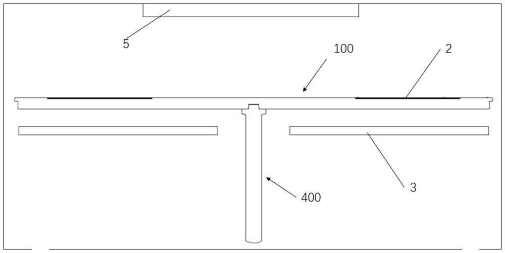
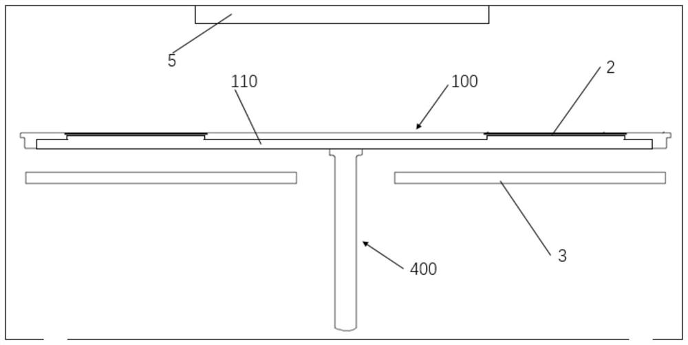
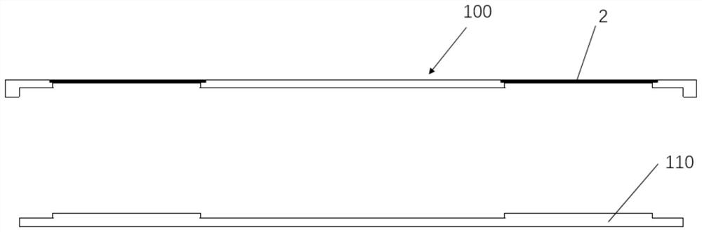
[0047] like figure 1 Shown is a schematic diagram of a reaction chamber used for deposition on a wafer surface in the prior art, including a reaction chamber, a gas shower head 5 is arranged at the top of the chamber, and an exhaust port is arranged at the bottom of the chamber, and the gas is sprayed from the gas. The shower head ...


PUM


Abstract

According to the wafer transmission cavity, the wafer and the tray are separated through cooperation of the supporting assembly and the wafer taking assembly, the wafer taking assembly can move up and down relative to the supporting assembly so as to support the wafer from the back face of the wafer to enable the wafer to be separated from the tray, the separated wafer can be conveniently placed into a wafer box by a follow-up mechanical arm, and meanwhile the wafer can be conveniently conveyed to the wafer box. Particle pollution caused by contact with the wafer from the edge of the front face is avoided, the uniform tracks of the supporting assembly and the wafer taking assembly are controlled through the system, the more stable and rapid wafer taking process can be achieved, and the overall efficiency can be improved.

Description

technical field [0001] The invention relates to the technical field of wafer deposition, in particular to the technical field of a wafer transfer chamber, a wafer deposition system and a wafer extraction method. Background technique [0002] Semiconductor devices, such as chips, go through a fabrication process in which microscopic circuits are formed on a silicon wafer as a substrate, which is then tested and packaged and divided into individual pieces. Among them, in the process of micro-circuit fabrication, it is necessary to deposit different material layers on the silicon wafer first as the basis for subsequent etching. In order to improve the deposition efficiency, in the deposition chamber, the process flow of taking advantage of multiple wafers at the same time is adopted, for example, in a circle A plurality of wafers are placed on a shaped tray, a heater is arranged behind the tray to heat the wafers, and deposition gas is introduced above the wafers. In general, ...

Claims


Application Information

Patent Timeline
Patent Type & Authority Applications(China)
IPC IPC(8): H01L21/67H01L21/677C23C16/458
CPCC23C16/458H01L21/67742H01L21/67766H01L21/67778H01L21/67196
Inventor 姜勇汪国元
Owner ADVANCED MICRO FAB EQUIP INC CHINA
Why Eureka
Try Eureka