

Preparation method for forming Split Gate MOSFET (Metal-Oxide-Semiconductor Field Effect Transistor) in one step
A conductivity type, trench technology, applied in semiconductor/solid-state device manufacturing, electrical components, circuits, etc., can solve problems such as increased manufacturing costs, increased manufacturing steps, and gatepoly residues
- Summary
- Abstract
- Description
- Claims
- Application Information
AI Technical Summary
Problems solved by technology
Method used
Image

Examples
Embodiment Construction
[0067] The technical solutions in the embodiments of the present invention will be clearly and completely described below with reference to the accompanying drawings in the embodiments of the present invention. Obviously, the described embodiments are only a part of the embodiments of the present invention, rather than all the embodiments. Based on the embodiments of the present invention, all other embodiments obtained by those of ordinary skill in the art without creative efforts shall fall within the protection scope of the present invention.
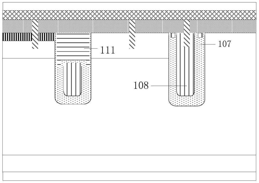
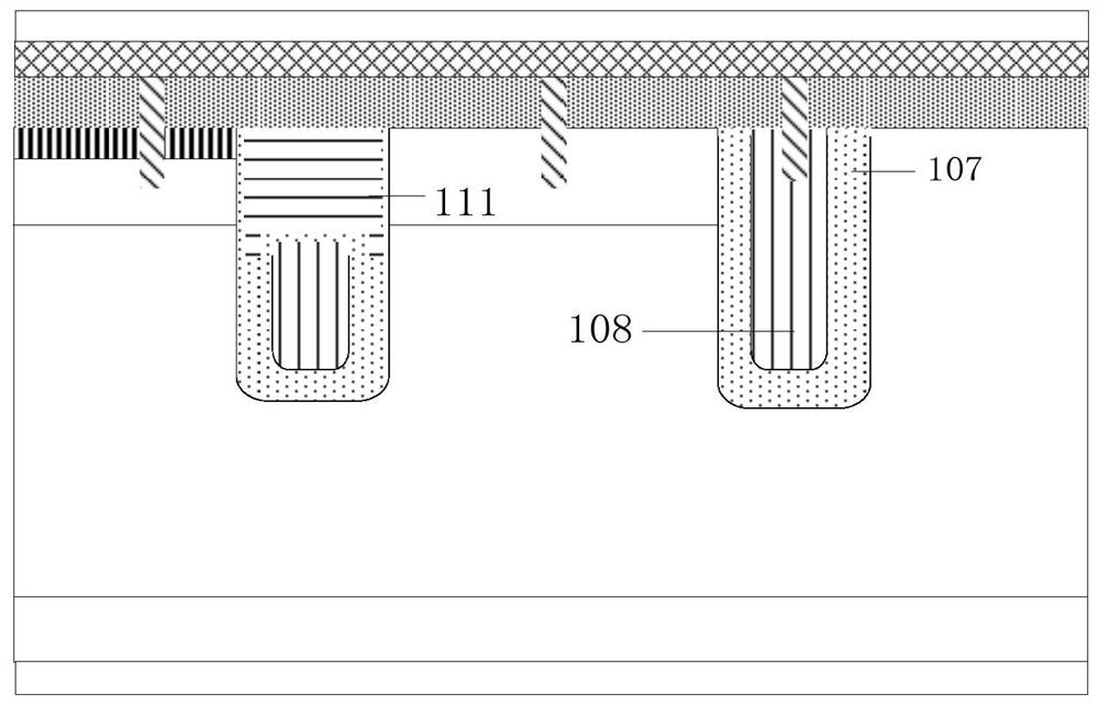
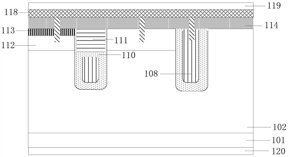
[0068] Figure 1C Illustratively shows a schematic structural diagram of a one-step Split Gate MOSFET device provided by an embodiment of the present invention, such as Figure 1C As shown, the one-step Split Gate MOSFET device mainly includes a first trench 105-1, a second trench 105-2, a first conductive epitaxial layer 102, a second conductive type body region 112, and a first conductive type source region 113, liner oxide layer ...
PUM
 Abstract
Description
Claims
Application Information