
Preparation method of Splitt-Gate MOSFET (Metal-Oxide-Semiconductor Field Effect Transistor) device

A device and trench technology, which is applied in the field of Split-Gate MOSFET device preparation, can solve the problems of restricting the growth trend of split-gate devices, large gate leakage of devices, and increased device costs.

Active Publication Date: 2022-03-01
华羿微电子股份有限公司
View PDF4 Cites 0 Cited by
  • Summary
  • Abstract
  • Description
  • Claims
  • Application Information

AI Technical Summary

Problems solved by technology

[0002] With the continuous maturity of process technology, Split-Gate MOSFET devices are gradually replacing Single Trench MOSFET devices in many fields. The production cost is still higher than that of Singlerench devices, thus restricting the growth trend of split-gate devices
However, the existing one-step forming process Split-GateMOSFET device manufacturing process has the following contradictions between cost saving and good device performance. First, if a layer of photomask is reduced in order to save costs, it will form gate poly residues on the top of the Source poly around the device. As a result, the device has a risk of excessive gate leakage, and if this risk is to be improved, it will inevitably increase the cost of the device

Method used


Image

  • Preparation method of Splitt-Gate MOSFET (Metal-Oxide-Semiconductor Field Effect Transistor) device
  • Preparation method of Splitt-Gate MOSFET (Metal-Oxide-Semiconductor Field Effect Transistor) device
  • Preparation method of Splitt-Gate MOSFET (Metal-Oxide-Semiconductor Field Effect Transistor) device

Examples


Embodiment Construction

[0059] The following will clearly and completely describe the technical solutions in the embodiments of the present invention with reference to the accompanying drawings in the embodiments of the present invention. Obviously, the described embodiments are only some, not all, embodiments of the present invention. Based on the embodiments of the present invention, all other embodiments obtained by persons of ordinary skill in the art without making creative efforts belong to the protection scope of the present invention.

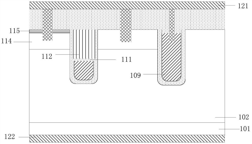
[0060] figure 1 It exemplarily shows a schematic structural diagram of a Split-Gate MOSFET device provided by an embodiment of the present invention, as figure 1 As shown, the Split-Gate MOSFET device mainly includes a first trench 107-1, a second trench 107-2, a first conductive epitaxial layer 102, a second conductive type body region 114, a first conductive type source region 115, liner oxide layer 108, source poly layer 109 and gate oxide layer 111.

[0...


PUM


Abstract

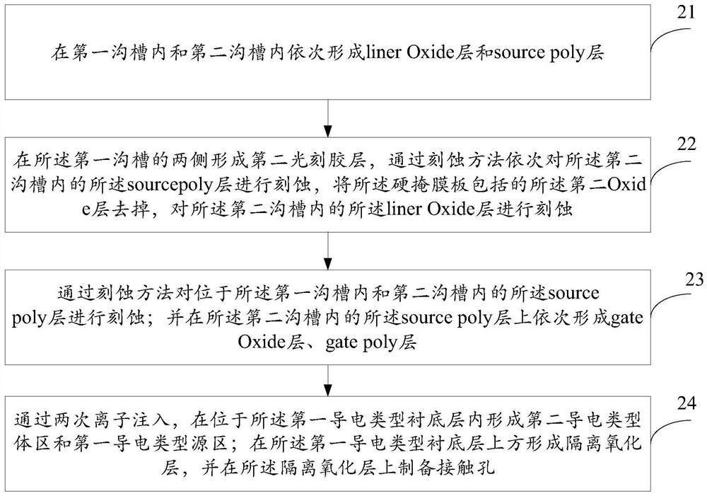
The invention discloses a preparation method of a Spit-Gate MOSFET (Metal-Oxide-Semiconductor Field Effect Transistor) device, and relates to the technical field of semiconductor power devices. The method is used for solving the problem that in the prior art, a forming process Splitt-Gate MOSFET device manufacturing process has contradiction between cost saving and good device performance. The preparation method comprises the following steps: sequentially forming a liner Oxide layer and a source poly layer in a first groove and a second groove; the source poly layer in the second groove is etched in sequence through an etching method, the second oxide layer included in the hard mask plate is removed, and the liner oxide layer in the second groove is etched; etching the source poly layer in the first groove and the source poly layer in the second groove through an etching method; a gate oxide layer and a gate poly layer are sequentially formed on the portion, in the second groove, of the source poly layer, and the gate oxide layer and the gate poly layer are sequentially formed on the portion, in the second groove, of the source poly layer; forming a second conductive type body region and a first conductive type source region through two times of ion implantation; and preparing a contact hole on the isolation oxide layer.

Description

technical field [0001] The invention relates to the technical field of semiconductor power devices, in particular to a method for preparing a Split-Gate MOSFET device. Background technique [0002] With the continuous maturity of process technology, Split-Gate MOSFET devices are gradually replacing Single Trench MOSFET devices in many fields. However, due to the difficulty of the process, the production cost is still higher than that of Singlerench devices, which restricts split-gate devices. growth trend. However, the existing one-step forming process Split-GateMOSFET device manufacturing process has the following contradictions between cost saving and good device performance. First, if a layer of photomask is reduced in order to save costs, it will form gate poly residues on the top of the Source poly around the device. As a result, the device has a risk of excessively large gate leakage, and if the risk is to be improved, the cost of the device will inevitably be increas...

Claims


Application Information

Patent Timeline
Patent Type & Authority Applications(China)
IPC IPC(8): H01L21/336H01L29/423
CPCH01L29/66477H01L29/4236
Inventor 袁力鹏苏毅杨科常虹
Owner 华羿微电子股份有限公司
Learn More