
Miniature light emitting diode packaging device and display panel

A technology for light-emitting diodes and packaging devices, which is applied in semiconductor devices, electric solid-state devices, electrical components, etc., can solve the problems of difficulty in preparing high-power quantum dot LEDs, a large number of quantum dot materials, and high cost, and achieves reduction of fluorescence quenching phenomenon, Improve luminous efficiency and reduce the effect of blue light components

Pending Publication Date: 2022-07-22
TCL CHINA STAR OPTOELECTRONICS TECH CO LTD
View PDF0 Cites 0 Cited by
  • Summary
  • Abstract
  • Description
  • Claims
  • Application Information

AI Technical Summary

Problems solved by technology

[0004] The embodiment of the present application provides a micro light-emitting diode packaging device and a display panel, which can solve the problem of requiring a large amount of quantum dot materials and high cost in the quantum dot LED of the prior art, and can solve the problem that it is difficult to prepare high-power quantum dot LEDs , can solve the problem of high blue light content

Method used


Image

  • Miniature light emitting diode packaging device and display panel
  • Miniature light emitting diode packaging device and display panel
  • Miniature light emitting diode packaging device and display panel

Examples


Embodiment 1

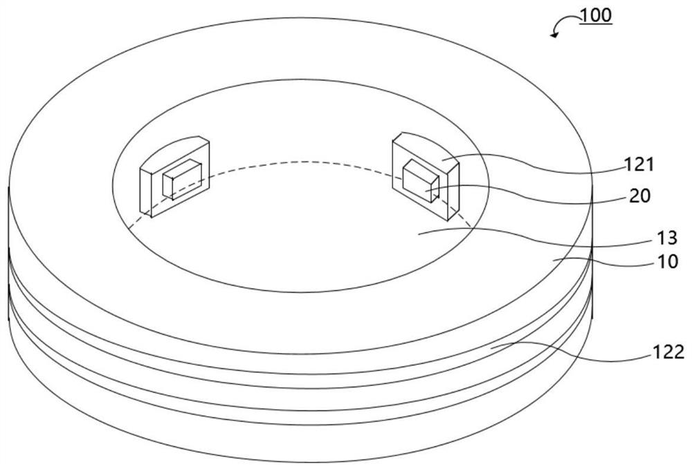
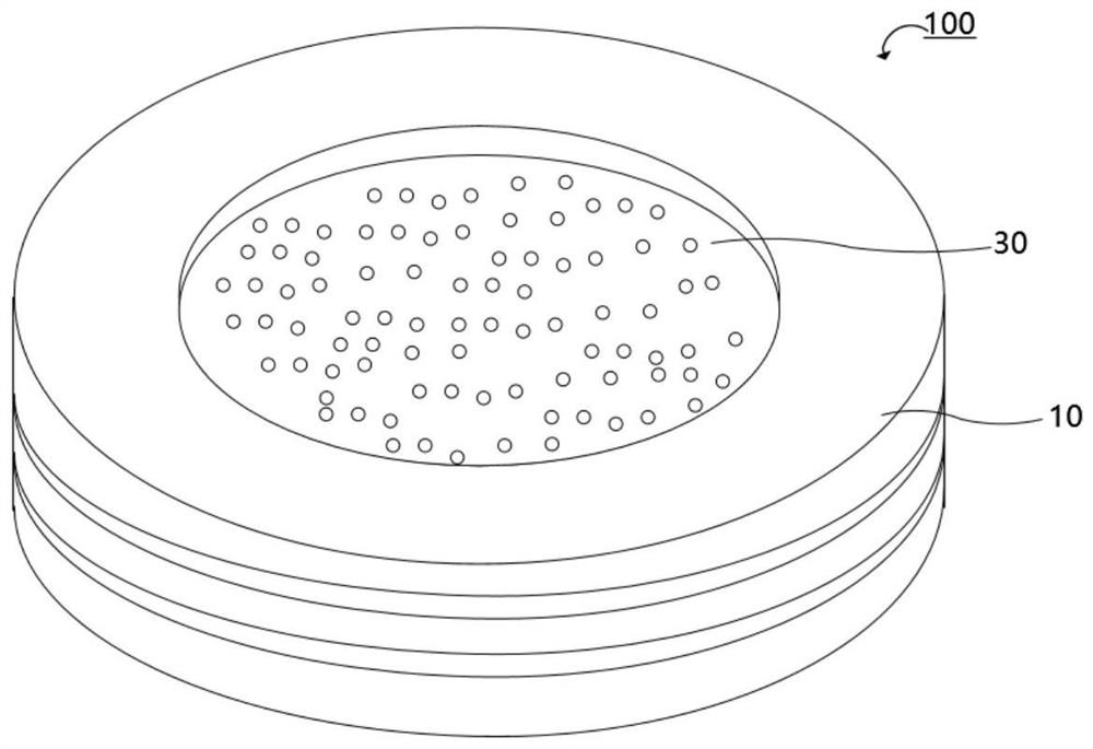
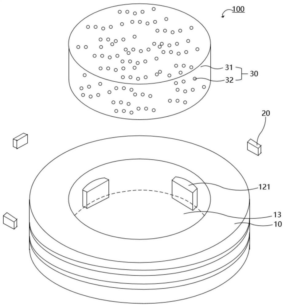
[0029] see Figure 1 to Figure 5 , figure 1 A schematic diagram of a first three-dimensional structure of a miniature light-emitting diode package device 100 provided in an embodiment of the present application; figure 2 A schematic diagram of a second three-dimensional structure of a miniature light-emitting diode package device 100 provided in an embodiment of the present application; image 3 An exploded view or exploded schematic diagram of a three-dimensional structure of a miniature light-emitting diode package device 100 provided in the embodiment of the present application; Figure 4 A schematic cross-sectional structure diagram of a miniature light-emitting diode package device 100 provided in an embodiment of the present application; Figure 5 This is a schematic diagram of a light emitting direction of a miniature light emitting diode package device 100 according to an embodiment of the present application. figure 1 The schematic diagram before the quantum dot l...

Embodiment 2

[0058] This embodiment is the same as or similar to the above-mentioned embodiment, except that the LED chip is disposed on the bottom wall.

[0059] In some embodiments, the LED chip 20 is disposed on the bottom wall 11 (not shown).

[0060] Specifically, the LED chip 20 is disposed on the bottom wall 11 in the accommodating cavity 13 , and also has the beneficial effects of the above-mentioned embodiments, which will not be repeated here.

Embodiment 3

[0062] This embodiment is the same as or similar to the above-mentioned embodiment, and the difference is that the light emitting process of the micro light emitting diode package device 100 is described.

[0063] Specifically, the quantum dots 32 may include green quantum dots, red quantum dots, or the quantum dots 32 may include white light quantum dots, but are not limited thereto.

[0064] Specifically, the LED chip 20 (light emitting diode chip) may be a blue LED chip, but is not limited thereto.

[0065] Specifically, one LED chip or a plurality of LED chips can be arranged in the accommodating cavity 13 , and the number of the LED chips is set according to the power requirement of the miniature light emitting diode package device 100 .

[0066] Specifically, as Figure 5 As shown, the LED chip 20 is a blue LED chip and the quantum dots 32 are green quantum dots as an example to illustrate the light-emitting process of the micro light-emitting diode package device of th...


PUM


Abstract

The invention discloses a miniature light-emitting diode packaging device and a display panel, and the miniature light-emitting diode packaging device comprises a housing which comprises an accommodation cavity; the at least one LED chip is fixedly arranged on the inner wall of the accommodating cavity; the quantum dot light-emitting layer is arranged in the accommodating cavity; wherein the quantum dot light-emitting layer comprises a rubber material body and doped quantum dots, and the light emitting direction of the LED chip faces the quantum dot light-emitting layer. The quantum dot light-emitting layer is arranged, the quantum dot light-emitting layer comprises the rubber material body and the doped quantum dots, the quantum dot materials are dispersed in the rubber material body, the quantum dot materials are not gathered, when the LED chip is converted through the quantum dot light-emitting layer, the fluorescence quenching phenomenon can be reduced, the light-emitting efficiency is improved, a high-power quantum dot LED is easily manufactured, and the light-emitting efficiency is improved. And when the LED chip is a blue light LED chip, the light emitted by the blue light LED chip is fully converted by the quantum dot light-emitting layer, so that the blue light component can be reduced.

Description

technical field [0001] The present application relates to the field of display, in particular to a miniature light emitting diode package device and a display panel. Background technique [0002] The birth of quantum dot LED (the combination of quantum dot material and miniature light-emitting diode) has undoubtedly injected new vitality and more scientific research impetus into the field of liquid crystal display panels. Due to its outstanding advantages in color gamut and color rendering index, quantum dot LEDs have brought more possible development directions to the flat panel display industry and provided users with rich color effects. At present, quantum dot display technology has entered mass production by preparing quantum dot thin film layers and combining them with LED backlights. [0003] However, currently, quantum dot LEDs are prepared by directly filling quantum dot materials when encapsulating LEDs. However, this method is still immature, requires a large amou...

Claims


Application Information

Patent Timeline
Patent Type & Authority Applications(China)
IPC IPC(8): H01L25/075H01L33/50H01L33/54H01L33/64
CPCH01L25/0753H01L33/507H01L33/54H01L33/64
Inventor 向昌明
Owner TCL CHINA STAR OPTOELECTRONICS TECH CO LTD
Learn More