Synchronous rectification driving circuit with low transmission delay
- Summary
- Abstract
- Description
- Claims
- Application Information
AI Technical Summary
Problems solved by technology
Method used
Image
Examples
Embodiment Construction
[0021] In order to make the purpose, technical solutions and advantages of the present application more clearly understood, the present application will be described in further detail below with reference to the accompanying drawings and embodiments. It should be understood that the specific embodiments described herein are only used to explain the present application, but not to limit the present application.
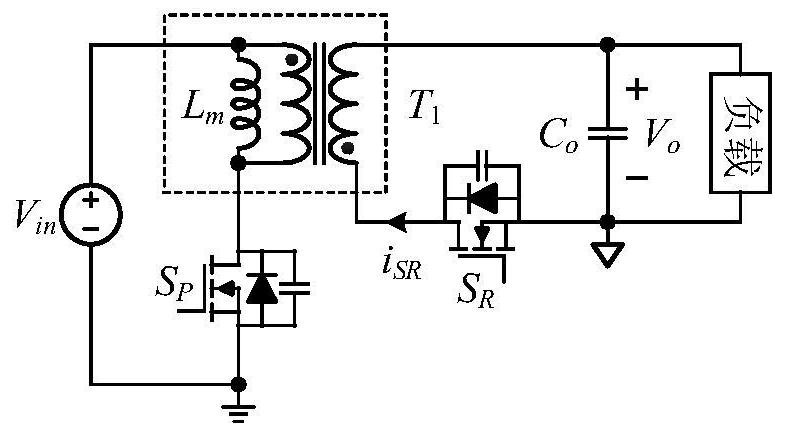
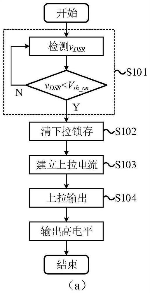
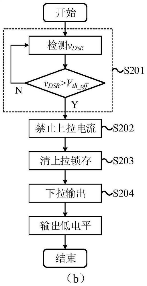
[0022]The present invention proposes a synchronous rectification drive circuit with low transmission delay. The system block diagram is as follows: Figure 4 As shown, it mainly includes a falling edge detection circuit, a pull-up current control circuit, a comparator CP1, an inverter N1, a single-pulse trigger circuit 1, a single-pulse trigger circuit 2, an RS flip-flop RS1, and a pull-up transistor Q. 1 and drop tube Q 2 . v in the figure D and v S Respectively, the synchronous rectifier S R The drain and source voltages of , and have v DSR =v D -v S , v IU_...
PUM
 Abstract
Description
Claims
Application Information
 - R&D
- Intellectual Property
- Life Sciences
- Materials
- Tech Scout
- Unparalleled Data Quality
- Higher Quality Content
- 60% Fewer Hallucinations
Browse by: Latest US Patents, China's latest patents, Technical Efficacy Thesaurus, Application Domain, Technology Topic, Popular Technical Reports.
© 2025 PatSnap. All rights reserved.Legal|Privacy policy|Modern Slavery Act Transparency Statement|Sitemap|About US| Contact US: help@patsnap.com


