
Trench gate semiconductor device

A trench gate and semiconductor technology, applied in semiconductor devices, electrical components, circuits, etc., can solve problems such as unreliable breakdown voltage performance

Pending Publication Date: 2022-07-29
NEXPERIA BV
View PDF0 Cites 0 Cited by
  • Summary
  • Abstract
  • Description
  • Claims
  • Application Information

AI Technical Summary

Problems solved by technology

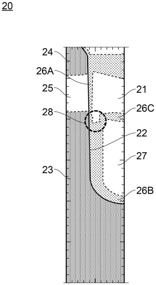
In other words, known devices are particularly sensitive to process variations when fabricated using known fabrication processes, and thus may be unreliable in terms of breakdown voltage performance between multi-trench MOSFET structures 20

Method used


Image

  • Trench gate semiconductor device
  • Trench gate semiconductor device
  • Trench gate semiconductor device

Examples


Embodiment Construction

[0044] Reference will be made below to the accompanying drawings. It should be noted that the same reference numbers may be used to refer to the same or similar parts. In addition, Figure 1 and Figures 2A to 2H The unit cells depicted in are symmetrical along the vertical axis in these figures. Therefore, for illustration purposes, only half of the unit cell is shown.

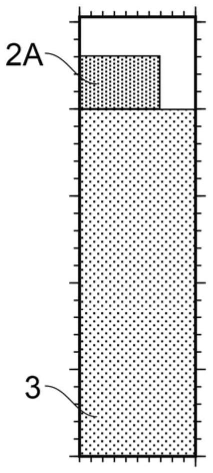
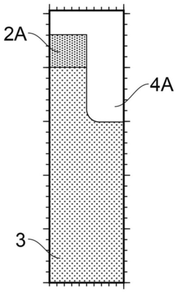
[0045] Figures 2A to 2H A first part of the process for fabricating the unit cell 1 of the trench gate semiconductor device 100 in which a silicon semiconductor region is used is shown. will refer to image 3 The remaining process steps are described. It should be noted that this process can be used to fabricate a single unit cell individually, or to fabricate multiple unit cells simultaneously on the same semiconductor region.

[0046] refer to Figure 2A , a first mask layer 2A is deposited and patterned onto the surface of the semiconductor region. For example, the first mask layer 2A is provided on ...


PUM

PropertyMeasurementUnit
lengthaaaaaaaaaa
widthaaaaaaaaaa

Abstract

The invention relates to a trench gate semiconductor device and a manufacturing method thereof. Each unit cell of the trench gate semiconductor device includes a first trench and a second trench extending from a bottom of the first trench. The semiconductor device further includes a gate oxide layer disposed on a first sidewall of the first trench; a second oxide layer disposed on a second sidewall and a bottom of the second trench; and a first polysilicon region disposed inside the first trench, the first polysilicon region being separated from the first sidewall by a gate oxide layer, and forming a gate of the unit cell. In addition, the semiconductor device includes: a second polysilicon region disposed inside the second trench, the second polysilicon region being separated from a second sidewall and a bottom of the second trench by a second oxide layer, and forming a buried source of the unit cell; and a third oxide layer disposed between the first polysilicon region and the second polysilicon region.

Description

technical field [0001] The present invention relates to trench gate semiconductor devices and methods of manufacturing the same. Background technique [0002] Trench technology for semiconductor devices such as trench metal oxide semiconductor field effect transistors (MOSFETs) is widely used in various types of electronic devices. In known trench MOSFETs, the gate electrode of the MOSFET is buried in a trench etched in the semiconductor region to form a vertical structure, which increases the channel density of the device. [0003] FIG. 1 shows a cross-sectional view of a portion of a known trench MOSFET structure 20 . The known device includes a polysilicon gate region 21 disposed in a trench 22 arranged inside a silicon semiconductor region. As shown in FIG. 1 , the semiconductor region comprises a substrate of the first charge type and an epitaxial layer 23 arranged on the substrate and also of the first charge type. Within the epitaxial layer 23, a body region 25 of ...

Claims


Application Information

Patent Timeline
Patent Type & Authority Applications(China)
IPC IPC(8): H01L29/423H01L29/78
CPCH01L29/4236H01L29/78H01L29/7813H01L29/407H01L29/41766H01L29/66727H01L29/66734H01L29/42364H01L29/42368
Inventor 史蒂文·皮克菲尔·鲁特
Owner NEXPERIA BV
Learn More