SNS Josephson junction based on VN and preparation method thereof
A technology of junction barrier and top electrode, which is applied in the field of superconducting electronics, can solve the problems of barrier regulation difficulty and unclear interface, and achieve the effect of adjustable resistivity, good uniformity and high interface flatness
- Summary
- Abstract
- Description
- Claims
- Application Information
AI Technical Summary
Problems solved by technology
Method used
Image
Examples
Embodiment 1
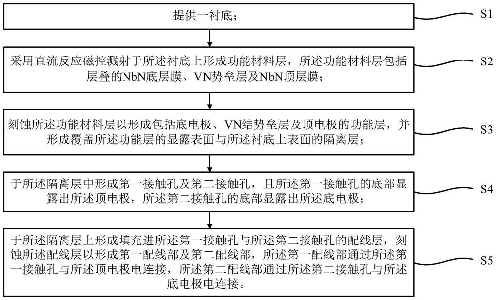
[0050] This embodiment provides a preparation method of an NbN-based SNS Josephson junction, such as figure 1 As shown, it is shown as a flow chart of the preparation method of the SNS Josephson junction, comprising the following steps:
[0051] S1: provide a substrate;
[0052] S2: adopting DC reactive magnetron sputtering to form a functional material layer on the substrate, and the functional material layer includes a stacked NbN bottom layer, a VN barrier layer and a NbN top layer;
[0053] S3: etching the functional material layer to form a functional layer including a bottom electrode, a VN junction barrier layer and a top electrode, and forming an isolation layer covering the exposed surface of the functional layer and the upper surface of the substrate;
[0054] S4: forming a first contact hole and a second contact hole in the isolation layer, and the top electrode is exposed at the bottom of the first contact hole, and the bottom electrode is exposed at the bottom of t...
Embodiment 2
[0088] This embodiment provides a VN-based SNS Josephson junction, such as Figure 9 As shown, it is a schematic diagram of the cross-sectional structure of the SNS Josephson junction, and the VN-based SNS Josephson junction is fabricated by the preparation method of the VN-based SNS Josephson junction described in the first embodiment.
[0089] Specifically, the SNS Josephson junction of the VN includes the substrate 1 , the functional layer 14 , the isolation layer 2 , the first wiring part 31 , the second wiring part 32 , the The first through hole 311 and the second through hole 321, wherein the functional layer 14 is located on the substrate 1, and the functional layer 14 includes the bottom electrode 111 stacked upward, the VN junction potential The barrier layer 121 and the top electrode 131, the isolation layer 2 covers the upper surface of the substrate 1 and the exposed surface of the functional layer 14, and the isolation layer 2 is provided with a bottom to expose ...
PUM
| Property | Measurement | Unit |
|---|---|---|
| diameter | aaaaa | aaaaa |
| thickness | aaaaa | aaaaa |
| thickness | aaaaa | aaaaa |
Abstract
Description
Claims
Application Information


