Superconducting integrated circuit with NbN SNS Josephson junction and preparation method thereof
An integrated circuit and superconducting technology, applied in the field of superconducting electronics, can solve the problems of low integration and difficulty in stable formation of superconducting digital integrated circuits, and achieve improved coverage and repeatability, area saving, and high industrial utilization value effect
- Summary
- Abstract
- Description
- Claims
- Application Information
AI Technical Summary
Problems solved by technology
Method used
Image
Examples
Embodiment 1
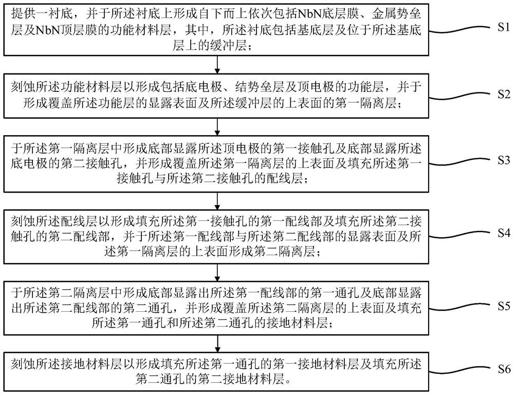
[0069] This embodiment provides a method for preparing a superconducting integrated circuit with a NbN SNS Josephson junction, such as figure 1 As shown, it is a flow chart of the preparation method for forming the NbN SNS Josephson junction, including the following steps:
[0070] S1: Provide a substrate, and form a functional material layer including a NbN bottom layer film, a metal barrier layer, and an NbN top layer film sequentially from bottom to top on the substrate, wherein the substrate includes a base layer and a A buffer layer on the base layer;
[0071] S2: Etching the functional material layer to form a functional layer including a bottom electrode, a junction barrier layer and a top electrode, and forming a first isolation layer covering the exposed surface of the functional layer and the upper surface of the buffer layer ;
[0072] S3: Form a first contact hole whose bottom exposes the top electrode and a second contact hole whose bottom exposes the bottom ele...
Embodiment 2
[0118] This embodiment provides a superconducting integrated circuit with NbN SNS Josephson junction, such as Figure 11 As shown, it is a schematic cross-sectional structure diagram of the superconducting integrated circuit with NbN SNS Josephson junction, and the superconducting integrated circuit with NbN SNS Josephson junction includes a substrate 1, a functional layer 24, a first isolation layer 3, The first wiring part 41, the second wiring part 42, the second isolation layer 5, the first grounding material layer 61 and the second grounding material layer 62, wherein the substrate 1 includes a base layer 11 and the buffer layer 12 on the base layer 11, the functional layer 24 is located on the upper surface of the buffer layer 12 and includes a bottom electrode 241, a junction barrier layer 242 and a top electrode 243 stacked upwards, the bottom The material of the electrode 241 includes NbN, the junction barrier layer 242 includes a metal barrier layer, the material of ...
PUM
| Property | Measurement | Unit |
|---|---|---|
| thickness | aaaaa | aaaaa |
| thickness | aaaaa | aaaaa |
| diameter | aaaaa | aaaaa |
Abstract
Description
Claims
Application Information


