

Service signal generating circuit
A technology of signal generation circuit and trigger circuit, which is applied in the direction of circuits, electrical components, information storage, etc., can solve the problems of inverter 104 voltage rise, inability to achieve low power consumption, and capacity increase, etc., to eliminate voltage fluctuations stable effect
- Summary
- Abstract
- Description
- Claims
- Application Information
AI Technical Summary
Problems solved by technology
Method used
Image

Examples
Embodiment 1
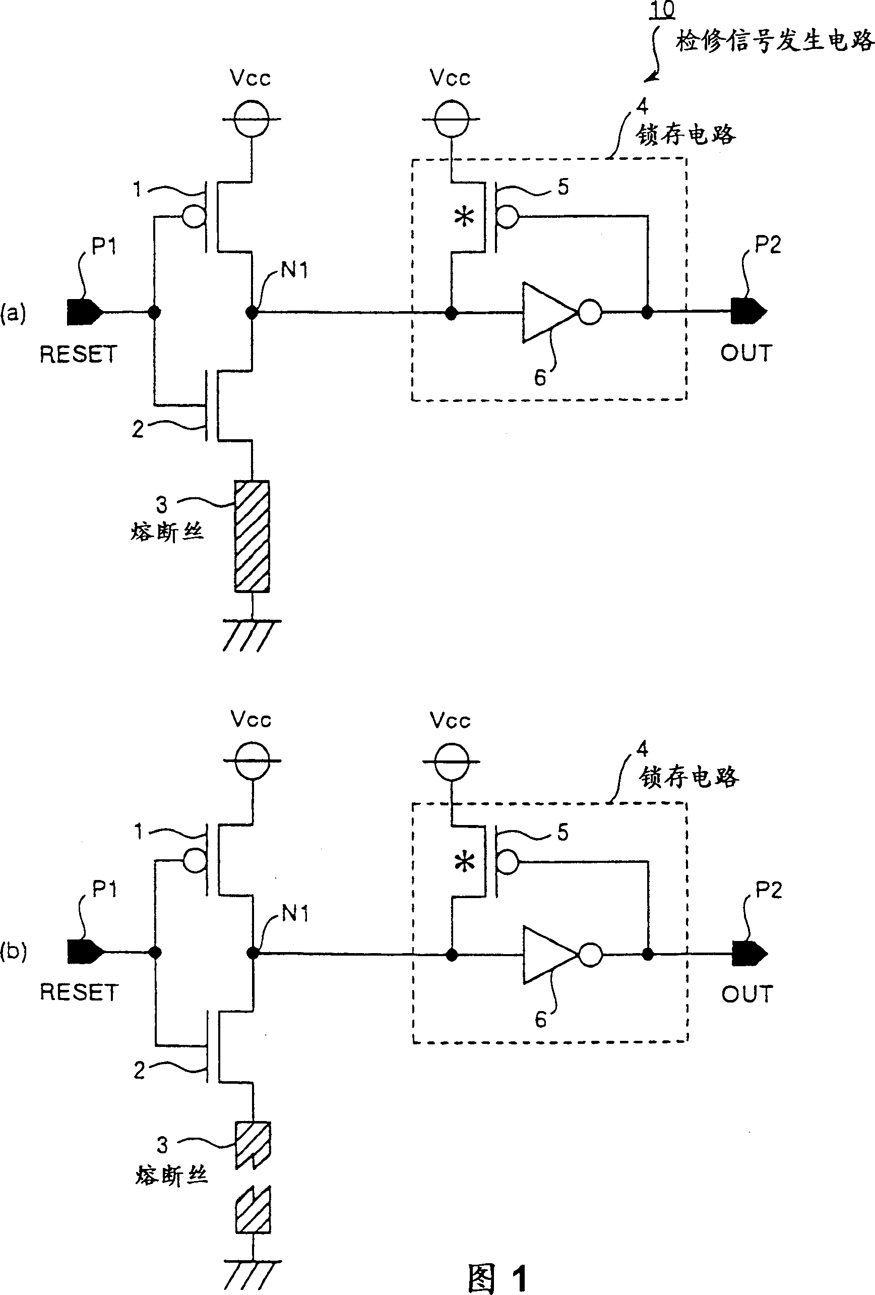
[0033] Fig. 1 is a circuit diagram showing the construction of a inspection signal generating circuit as Embodiment 1 of the present invention. In FIG. 1, a source of a p-channel transistor 1 is connected to a power supply Vcc, and a reset signal "RESET" is input to a gate from a terminal P1. The source of the n-channel transistor 2 is connected to the grounded fuse 3, the drain is connected to the drain of the p-channel transistor 1, and a reset signal "RESET" is input to the gate from the terminal P1.
[0034] The input side of the inverter 6 is connected to the node N1 which is the connection point of the p-channel transistor 1 and the n-channel transistor 2, and the output of the inverter 6 outputs the inspection signal "OUT" via the terminal P2. The source of p-channel transistor 5 is connected to power supply Vcc, the drain is connected to node N1 , and the gate is connected to the output side of inverter 6 . The drive capability of the p-channel transistor 5 is lower tha...
Embodiment 2
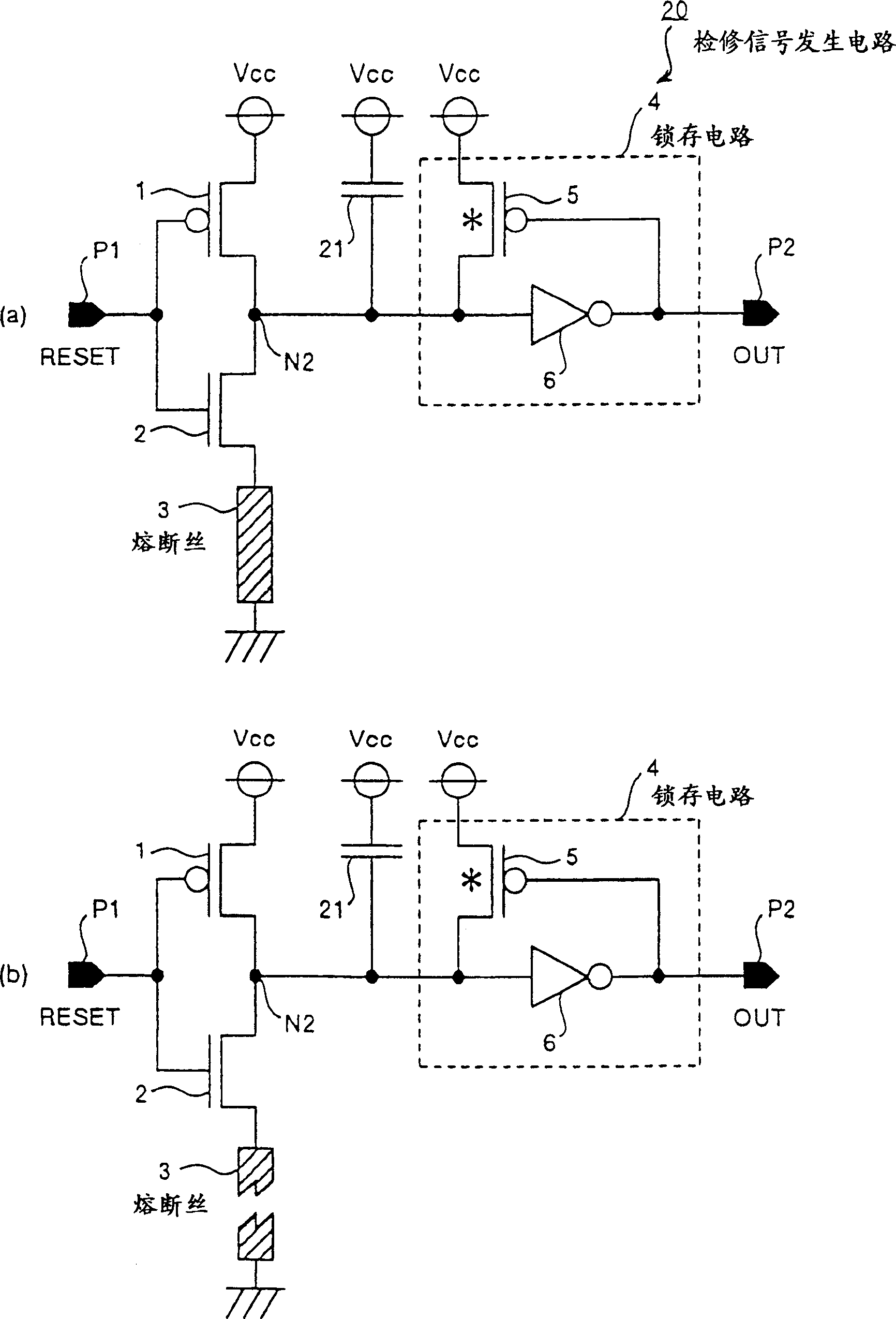
[0048] Next, Embodiment 2 of the present invention will be described. In this second embodiment, a capacitor is provided for stabilizing the voltage level of the node N1 of the inspection signal generating circuit 10 shown in FIG. 1 for a constant period.
[0049] figure 2 It is a circuit diagram showing the structure of the inspection signal generating circuit as the second embodiment of the present invention. figure 2 (a) shows the structure of the inspection signal generating circuit in a state where the fuse 3 is not cut, figure 2 (b) shows the configuration of the inspection signal generating circuit in a state where the fuse 3 is cut. figure 2 The inspection signal generating circuit 20 shown in FIG. 1 adopts a structure in which a capacitor 21 is further connected between a node N2 corresponding to the node N1 of the inspection signal generating circuit 10 shown in FIG. 1 and a power supply Vcc. By providing this capacitor 21, the potential change of the node N2 can ...
Embodiment 3
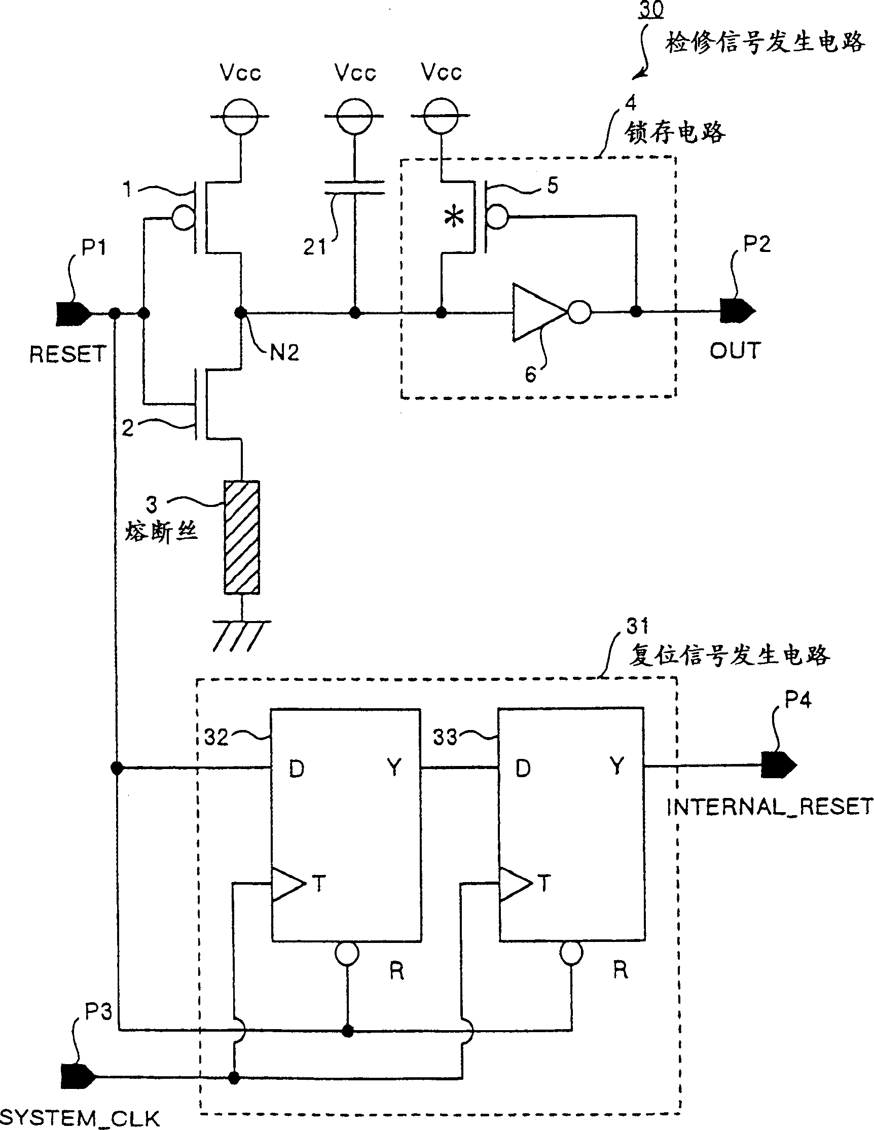
[0060] Next, Embodiment 3 of the present invention will be described. In this Embodiment 3, after the inspection signal supplied by the inspection signal generating circuit is determined, a reset signal indicating reset release is supplied to other circuits on the semiconductor integrated circuit mounted with the inspection signal generating circuit, so that the The timing-critical operation is caused by the competition between the inspection operation of the inspection signal and the reset release operation of other circuits on the semiconductor integrated circuit.
[0061] image 3 It is a circuit diagram showing the structure of the inspection signal generating circuit as the third embodiment of the present invention. image 3 The maintenance signal generation circuit 30 shown in the figure 2 The structure of the reset signal generating circuit 31 is added to the inspection signal generating circuit 20 shown in .
[0062] The reset signal generating circuit 31 has two fl...
PUM
 Abstract
Description
Claims
Application Information