Structure and read-write method of double-bit non-volatile memory unit
A non-volatile storage, dual-bit technology, applied in electrical components, electrical solid-state devices, circuits, etc., can solve the problems of prone to errors, increase the difficulty of operating memory, inconsistent electrical properties of memory cells, etc., to reduce the area. Effect
- Summary
- Abstract
- Description
- Claims
- Application Information
AI Technical Summary
Problems solved by technology
Method used
Image

Examples
Embodiment Construction
[0034] The structure of the double-bit non-volatile memory cell of the preferred embodiment of the present invention, two programming methods, and its reading method will be described in sequence below, and this kind of double-bit non-volatile memory cell can be used in a flash memory, for example. In the memory (Flash Memory).
[0035] Structure of a dual-bit non-volatile memory cell
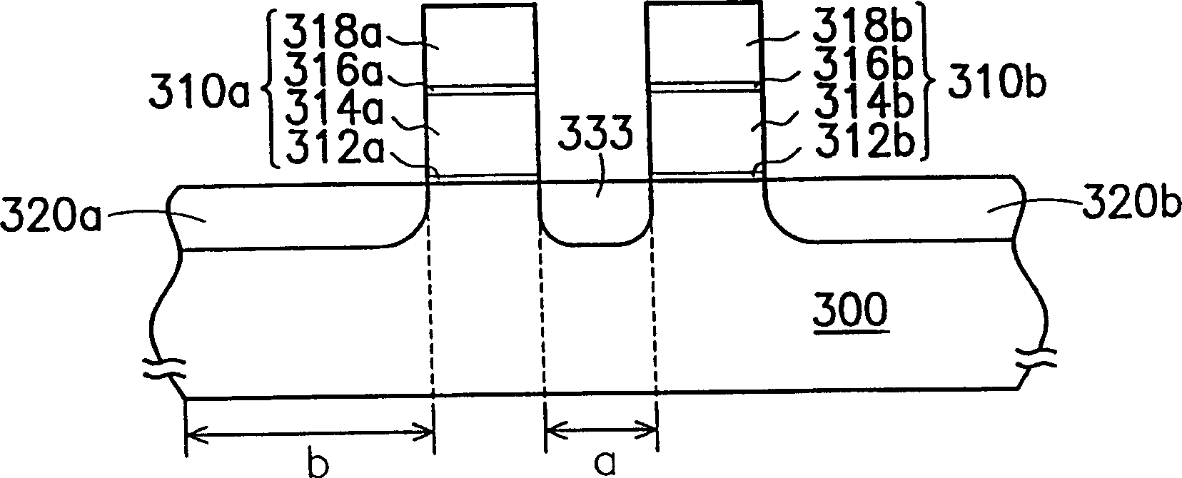
[0036] Please refer to image 3, which shows the structure of the dual-bit non-volatile memory unit of the preferred embodiment of the present invention. Such as image 3 As shown, the memory cell includes a substrate 300 , two stacked gate structures 310 a and 310 b , source / drain regions 320 a and 320 b , and a doped region 333 . Wherein, the stacked gate structure 310a / b includes tunnel oxide layer 312a / b, floating gate 314a / b, inter-gate dielectric layer 316a / b and control gate 318a / b stacked from bottom to top; doped region 333 Located in the substrate 300 between the stacked gate st...
PUM
 Abstract
Description
Claims
Application Information
 - R&D Engineer
- R&D Manager
- IP Professional
- Industry Leading Data Capabilities
- Powerful AI technology
- Patent DNA Extraction
Browse by: Latest US Patents, China's latest patents, Technical Efficacy Thesaurus, Application Domain, Technology Topic.
© 2024 PatSnap. All rights reserved.Legal|Privacy policy|Modern Slavery Act Transparency Statement|Sitemap