Crystal covered chip and crystal covered package substrate

A technology for packaging substrates and flip chips, which is applied to electrical components, electrical solid-state devices, circuits, etc., can solve the problems of increasing the length of the signal transmission path, reducing the electrical performance of the chip 110, and increasing the line length of the chip 110.

Inactive Publication Date: 2004-12-01
VIA TECH INC
View PDF0 Cites 0 Cited by
  • Summary
  • Abstract
  • Description
  • Claims
  • Application Information

AI Technical Summary

Problems solved by technology

It should be noted that, since the known signal pads 114a, power pads 114b and ground pads 114c are irregularly distributed on the active surface 112 of the chip 110, when the original pads on the chip 110 (not (shown) When redistributed on the active surface 112 of the chip 110 through the redistribution layer (...

Method used


Image

  • Crystal covered chip and crystal covered package substrate
  • Crystal covered chip and crystal covered package substrate
  • Crystal covered chip and crystal covered package substrate

Examples


Embodiment Construction

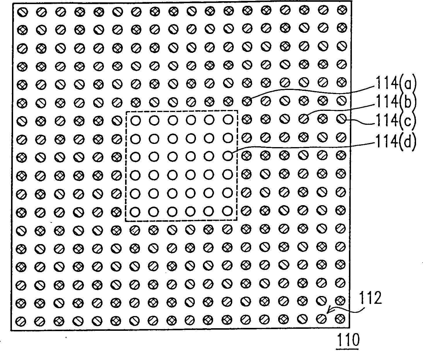
[0044] Please refer to Figure 3A , which is a bottom view of a chip in a preferred embodiment of the present invention. The active surface 212 of the chip 210 is provided with a plurality of bonding pads 214 (such as component numbers 214 a , 214 b , 214 c , 214 d . . . ) in a matrix, forming a plurality of bonding pad rings 215 . In addition, according to different functions, the pads 214 can also be divided into signal pads 214a, power pads 214b, ground pads 214c, and core power / ground pads 214d, wherein the signal pads 214a, power pads 214b and ground pads The pads 214c are centered on the core power / ground pads 214 and distributed around the core power / ground pads 214d. It should be noted that, for a signal pad ring composed of a plurality of pads 214 (such as the second pad ring 215b, the third pad ring 215c and the sixth pad ring 215f), the pads 214 have 100% More than 50% are signal pads 214a, and preferably, more than 90% of the pads 214 of the signal pad ring are s...


PUM


Abstract

A crystal covered chip consists of several core powder sources and earthing weld pads, at least one signal weld pad ring, at least one power source weld pad ring and at least one earthing weld pad ring, all of which are configurated on the active surface of the crystal covered chip and the said weld pad rings are distributed in concentric ring like around the periphery of these earthing weld pads for core powder sources by using these core power sources/earthing weld pads as a centre. In addition, a crystal covered packaging substrate has several lug pads at the most top layer of wire layers, which has the positions corresponding to the positions of weld pads for the crystal covered chip seperately. A lug pad ring of nonsignal can be configurated at the periphery of lug pad ring and a pair of power source trace or earthing trace as the protective trace for signal trace can be configurated at both sides of a signal trace separately on an any wire layer in the crystal covered packaging substrate.

Description

technical field [0001] The present invention relates to a flip chip and a flip chip package substrate, and more particularly to a flip chip with a plurality of pad rings, and a flip chip corresponding to the above flip chip with a plurality of bumps. Flip Chip Package Substrate with Block Spacer Ring. Background technique [0002] Flip Chip bonding technology (Flip Chip, FC) is a common chip packaging technology used in chip scale packaging (Chip Scale Package, CSP), which mainly uses the arrangement of the area array (Area Array), the chip ( A plurality of die pads of die) are designed to be arranged on the active surface of the chip (active surface), that is, the side of the chip with active components (active device), and bumps (bumps) are respectively formed on each pad, and then Then, the bumps on the chip are connected to the corresponding contacts on the carrier, so that the chip is correspondingly bonded to the surface of the carrier in a flipping manner. [0003] ...

Claims


Application Information

Patent Timeline
IPC IPC(8): H01L23/14H01L23/50
CPCH01L2224/10
Inventor 许志行
Owner VIA TECH INC
Why Eureka
Try Eureka