Process for preparing low storage junctions of DRAM

A technology of thin film layer and photoresist layer, which is applied to the original parts, instruments, and optomechanical equipment used for photomechanical processing, and can solve the problems affecting the electrical performance of integrated circuits and reducing the power of the storage junction 30 under the capacitor, etc. Achieve the effects of improving optical proximity effect, solving circular deformation and shrinkage, and increasing power storage

Inactive Publication Date: 2004-12-08
UNITED MICROELECTRONICS CORP
View PDF0 Cites 0 Cited by
  • Summary
  • Abstract
  • Description
  • Claims
  • Application Information

AI Technical Summary

Problems solved by technology

Because the size of the photoresist pattern 26 is smaller than the original design pattern ( image 3 The pattern indicated by the dotted line in the figure), so that the size of the subsequently formed capacitor lower storage junction 30 is smaller than the original design size, thereby reducing the amount of electricity that can be stored by the capacitor lower storage junction 30 and affecting the electrical performance of the integrated circuit

Method used


Image

  • Process for preparing low storage junctions of DRAM
  • Process for preparing low storage junctions of DRAM
  • Process for preparing low storage junctions of DRAM

Examples


Embodiment Construction

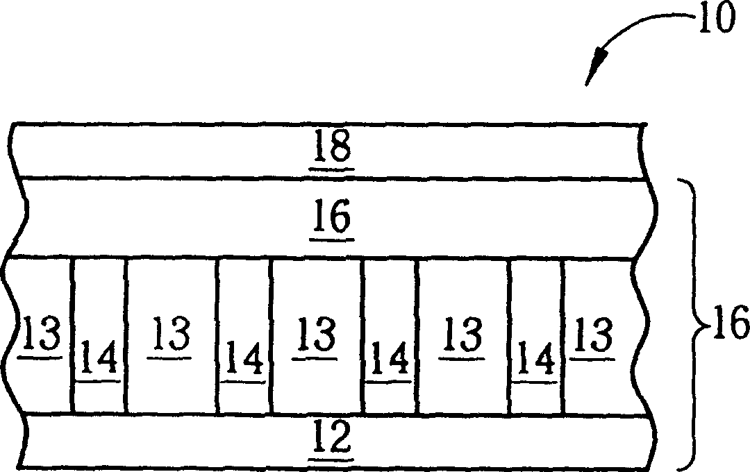
[0055] refer to Figure 10 to Figure 14 , Figure 10 to Figure 14 It is a schematic diagram of the photolithography process according to the present invention. The photolithography process is used to pattern the size and location of the capacitive lower storage junctions of the DRAM on a semiconductor wafer 60 . Such as Figure 10 As shown, the semiconductor wafer 60 includes a silicon substrate 62, an insulating layer 63 made of a silicon oxide compound is arranged on the surface of the silicon substrate 62, and a plurality of contact junctions 64 made of doped polysilicon are arranged in the insulating layer 63, A polysilicon or amorphous silicon layer 65 for forming the underlying storage junction is disposed on the surface of the insulating layer 63 and covers the contact junctions 64 , and a photoresist layer 67 is disposed on the surface of the semiconductor wafer 60 . Wherein, the contact junction 64 is used to electrically connect a drain (not shown) of a MOS transi...


PUM


Abstract

The ivnention relates to the method for manufacturing the low layer memory node of the Dynamic Random Access Memory (DRAM) on the semiconductor water. The semiconductor wafer includes the substrate, the thin field layer and photoresist layer. The two exposures are carried out on the photoresist layer above the thin film layer. The first exposure area with multiple strips paralleled is formed at the first exposure. The second exposure forms the second exposure area in tesselation. After develop, the photoresist layer in the first and second exposure areas is removed so as to form the array type photoresist layer, which is used as the mask for etching the thin film layer, on the surface of the thin film layer. After being etched, the thin film is in array distribution, which can be used as the low layer memory node of DRAM.

Description

technical field [0001] The invention provides a method for fabricating a lower storage junction of a DRAM, in particular a method for fabricating a DRAM lower storage junction which avoids pattern deformation due to optical proximity effects. Background technique [0002] Photolithography is the most important step in the semiconductor process, which can smoothly transfer the layout pattern of integrated circuits to the semiconductor wafer. In order to form a designed integrated circuit on a semiconductor wafer, the fab must first make a photomask (reticle) and form a designed pattern on the photomask, and then use the development process to convert the photomask The pattern on the semiconductor wafer is transferred to the photoresist layer on the surface of the semiconductor wafer in a certain proportion. [0003] With the continuous improvement of the complexity and integration of integrated circuits, the patterns on the illumination are also designed to be smaller and sm...

Claims


Application Information

Patent Timeline
Patent Type & Authority Patents(China)
IPC IPC(8): G03F1/56G03F7/00H01L21/027H01L21/28H01L21/8242
Inventor 黄俊仁陈桂顺黄义雄
Owner UNITED MICROELECTRONICS CORP
Why Eureka
Try Eureka