Silicon insulator structure simicoductor device

A semiconductor and device technology, applied in the field of SOI structure semiconductor devices, can solve the problems of reduced efficiency, narrow process margin, and complicated manufacturing process.

Inactive Publication Date: 2005-02-23
SHARP KK
View PDF0 Cites 0 Cited by
  • Summary
  • Abstract
  • Description
  • Claims
  • Application Information

AI Technical Summary

Problems solved by technology

[0023] However, due to this structure, when a fully depleted device with a gate length of 0.25 microns is required, for example, the process margin for forming the im...

Method used


Image

  • Silicon insulator structure simicoductor device
  • Silicon insulator structure simicoductor device
  • Silicon insulator structure simicoductor device

Examples


Embodiment 1

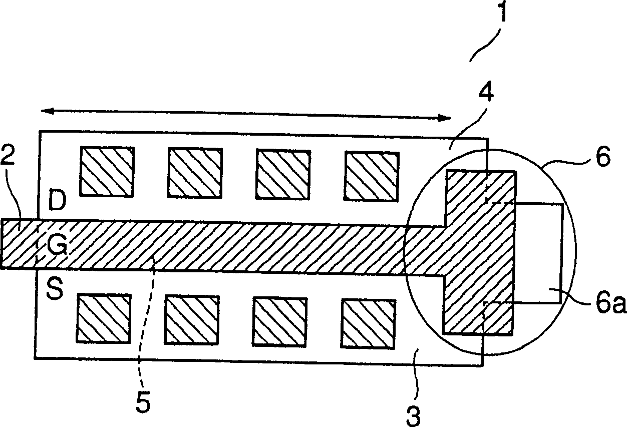
[0053] As shown in Figure 1(a), the SOI MOSFET in this embodiment is fabricated on an SOI substrate. The SOI substrate is a buried oxide film with a thickness of about 120nm and a surface silicon layer with a thickness of about 50nm. The way it is constructed on the substrate. The LOCOS film 1 is formed on the surface silicon layer of the SOI substrate to define the active area. The gate 2 doped with N-type impurities is formed on the active region by a gate oxide film with a thickness of about 7 nm, and the gate length L=0.35 μm. In addition, the N-type source region 3 and the drain region 4 are formed in those surface silicon layer portions on both sides of the gate 2. By the way, the surface silicon layer is in a floating state.

[0054] The channel region 5 is formed directly below the gate 2, and the potential well 6 is formed directly below the channel region 5 in the gate width direction (the direction indicated by the arrow in FIG. 1(a)), and surrounds the channel region 5...

Embodiment 2

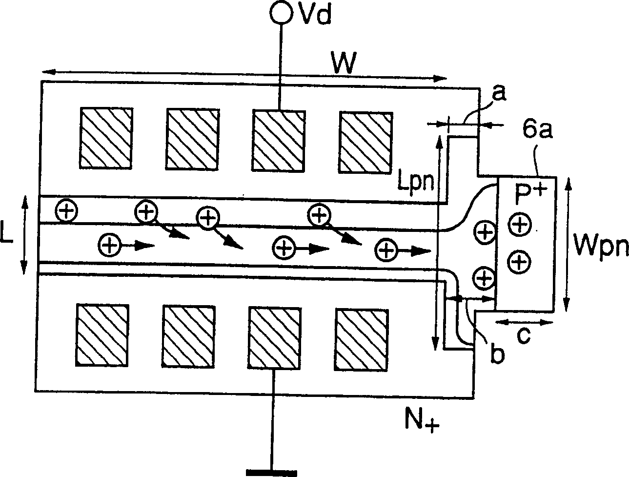
[0069] Such as Figure 4 As shown, except that the potential wells 6 are formed on both sides of the channel region 5, the SOI MOSFET in this embodiment is basically the same as the SOI MSOFET in the first embodiment.

[0070] Therefore, the holes generated near the drain junction will migrate to the two potential wells 6.

Embodiment 3

[0072] Such as Figure 5 As shown, except that the potential well 16 is formed directly below both ends of the channel region 5 in the direction of its gate width, and does not include any protruding active regions or any regions with higher impurity concentration, the SOIMOSFET of this embodiment is compatible with The SOI MOSFET of Embodiment 1 is basically the same.


PUM


Abstract

A semiconductor device of SOI structure comprises a surface semiconductor layer in a floating state, which is stacked on a buried insulating film so as to construct an SOI substrate, source/drain regions of second conductivity type which are formed in the surface semiconductor layer, a channel region of first conductivity type between the source/drain regions and a gate electrode formed on the channel region through a gate insulating film; wherein the surface semiconductor layer has a potential well of the first conductivity type formed therein at and/or near at least one end of the channel region in a gate width direction thereof.

Description

Technical field [0001] The present invention relates to a semiconductor device with a silicon insulator (SOI) structure, and in particular to a semiconductor device with an SOI structure that reduces the "bending effect". Background technique [0002] MOSFETs manufactured on commonly known SOI structures such as SOS, SIMOX or BSOI substrates can operate at low voltage and high speed. In addition, compared with devices manufactured on bulk silicon substrates, SOI MOSFETs have the advantage of achieving a smaller layout area. [0003] At the same time, although bulk silicon MOSFETs have four terminals (gate, drain, source, and substrate), SOI MOSFETs have only three terminals (gate, drain, and source). Therefore, the SOI MOSFET will degrade the electrical characteristics of the device, especially the short channel effect and the breakdown voltage between the drain and the source. [0004] More specifically, in a bulk silicon MOSFET, as shown in Figures 7(a) and 7(b), a parasitic bi...

Claims


Application Information

Patent Timeline
IPC IPC(8): H01L27/12H01L21/84H01L29/78H01L29/786
CPCH01L29/7841H01L29/78612H01L29/78696H01L2924/0002H01L2924/00H01L21/84H01L27/12H01L29/78
Inventor A·O·阿丹
Owner SHARP KK
Why Eureka
Try Eureka