
Dye-sensitized photoelectric conversion device module, method for manufacturing the same, and electronic device

A technology of photoelectric conversion elements and dyes, which can be used in electrical components, photovoltaic power generation, battery electrodes, etc., and can solve the problems of low photoelectric conversion efficiency of solar cells

Inactive Publication Date: 2010-03-17
SONY CORP
View PDF0 Cites 3 Cited by
  • Summary
  • Abstract
  • Description
  • Claims
  • Application Information

AI Technical Summary

Problems solved by technology

However, the photoelectric conversion efficiency of such solar cells is very low, equal to or less than 1%, and there is also a problem of durability

Method used


Image

  • Dye-sensitized photoelectric conversion device module, method for manufacturing the same, and electronic device
  • Dye-sensitized photoelectric conversion device module, method for manufacturing the same, and electronic device
  • Dye-sensitized photoelectric conversion device module, method for manufacturing the same, and electronic device

Examples


Embodiment 1

[0064] After the FTO film was formed on the glass substrate, the FTO film was patterned into 8 stripe patterns by etching such that a gap with a width of 0.5 mm was defined between every 2 stripe patterns. Thereafter, ultrasonic cleaning is performed using acetone, alcohol, an alkaline cleaning solution, and ultrapure water in this order, and drying is sufficiently performed.

[0065] Titanium oxide paste made of Solaronix was applied onto a glass substrate by using a screen printing machine so as to obtain 8 stripe patterns each having a width of 5 mm and a length of 40 mm (a total area of ​​16 cm 2 ). Regarding the paste, a transparent Ti-Nanoxide TSP paste and a Ti-Nanoxide DSP containing scattering particles therein were sequentially laminated from the glass substrate side so as to have a thickness of 7 μm and a thickness of 13 μm, respectively. As a result, porous TiO with a total thickness of 20 μm was obtained 2 membrane. Firing porous TiO in an electric furnace at 5...

Embodiment 2

[0075] A dye-sensitized photoelectric conversion element module was manufactured similarly to the case of Example 1 except that the carbon paste for the counter electrode was formed into a foil shape.

Embodiment 3

[0077] A dye-sensitized photoelectric conversion element module was fabricated similarly to the case of Example 1 except that the counter electrode was formed into a foil shape with platinum-supported carbon paste.


PUM

PropertyMeasurementUnit
melting pointaaaaaaaaaa
thicknessaaaaaaaaaa
diameteraaaaaaaaaa

Abstract

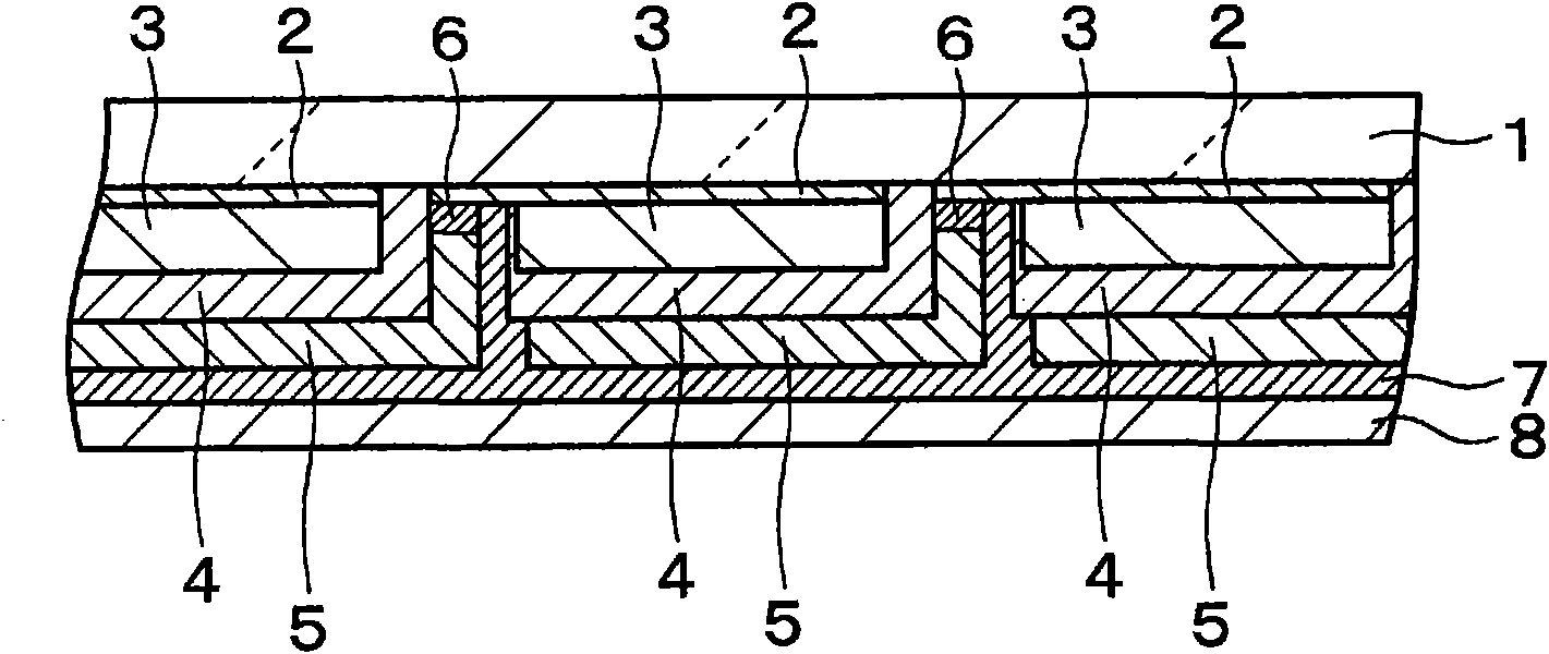
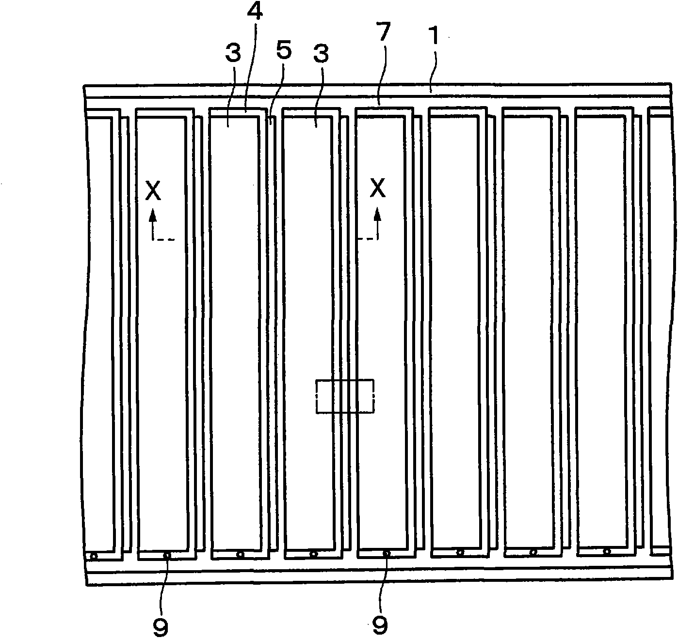
A dye-sensitized photoelectric conversion device is formed by sequentially arranging a dye-sensitized semiconductor layer (3), a porous insulating layer (4) and a counter electrode (5) on a transparent conductive layer (2) which is formed on a transparent substrate (1). The counter electrode (5) is composed of a metal or alloy foil having a catalyst layer on one surface which is on the porous insulating layer (4) side, or a foil made of a material having a catalytic activity. At a position between two adjacent dye-sensitized photoelectric conversion devices, the transparent conductive layer (2) of one dye-sensitized photoelectric conversion device and the counter electrode (5) of the other dye-sensitized photoelectric conversion device are electrically connected with each other. The dye-sensitized semiconductor layer (3) and the porous insulating layer (4) are impregnated with an electrolyte.Each dye-sensitized photoelectric conversion device is covered with a sealing layer (7).

Description

technical field [0001] The present invention relates to a dye-sensitized (sensitized) photoelectric conversion element module, a manufacturing method thereof, and an electronic device, and for example, the present invention is suitably applied to a dye-sensitized semiconductor layer made of dye-loaded semiconductor fine particles dye-sensitized solar cells, and various electronic devices. Background technique [0002] It is considered that when a fossil fuel such as coal or petroleum is used as an energy source, global warming is caused because carbon dioxide is generated due to the use of the fossil fuel. In addition, the application of nuclear energy has a great risk of pollution due to nuclear radiation. Currently, when people talk about environmental issues, there are many problems with the dependence on these energy sources. [0003] On the other hand, a solar cell, which is a photoelectric conversion element for converting sunlight into electrical energy, exerts an e...

Claims


Application Information

Patent Timeline
Patent Type & Authority Applications(China)
IPC IPC(8): H01M14/00H01L31/04H01M2/22H01M50/528
CPCH01G9/2022Y02E10/542H01G9/2059Y02T10/7022H01M4/9041H01G9/2013H01G9/2081Y02E60/50H01M14/005H01G9/2031Y02P70/50Y02T10/70H01L31/042
Inventor 诸冈正浩铃木祐辅米屋丽子
Owner SONY CORP
Learn More