
Semiconductor laser device and optical pick-up apparatus using semiconductor laser device

A technology of lasers and semiconductors, which is applied to semiconductor lasers, structural details of semiconductor lasers, semiconductor devices, etc., can solve problems such as difficulty in maintaining bonding strength, difficulty in ensuring positional accuracy, and complicated processes, and achieve good heat dissipation, low performance, and The effect of stable performance

Inactive Publication Date: 2005-05-11
PANASONIC CORP
View PDF3 Cites 1 Cited by
  • Summary
  • Abstract
  • Description
  • Claims
  • Application Information

AI Technical Summary

Problems solved by technology

Therefore, there is a problem that it is difficult to achieve both miniaturization and high functionality
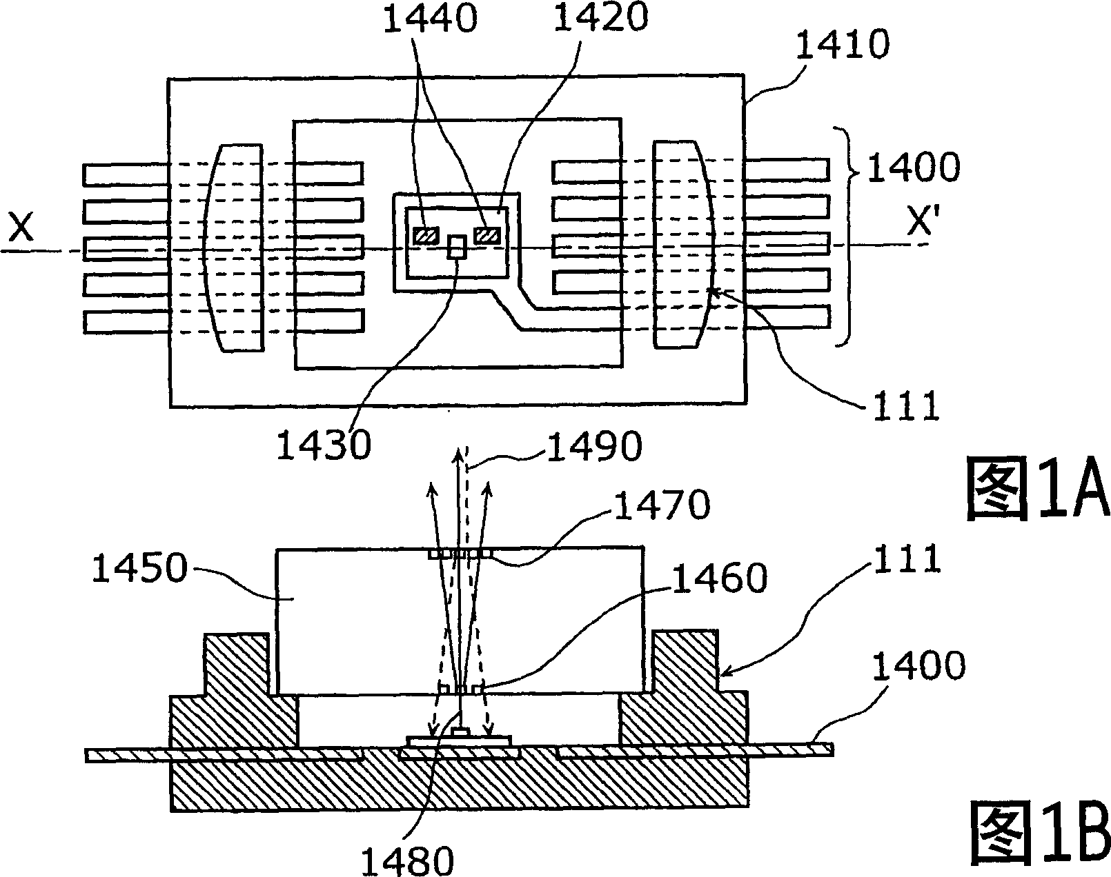
Furthermore, the above-mentioned Japanese Patent Application Laid-Open No. 2003-67959 does not describe a semiconductor laser module having an optical element such as a diffraction grating. However, using the semiconductor laser assembly described in the above-mentioned Japanese Patent Application Laid-Open No. 2003-67959, there is a problem that the optical element cannot be bonded and fixed on the package.
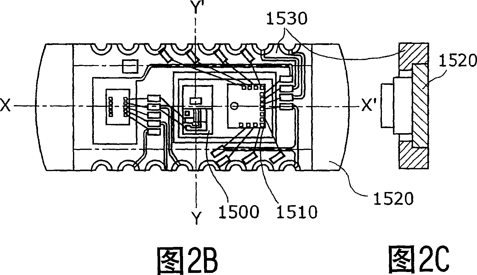
[0019] In addition, in the semiconductor laser module described in the above-mentioned Japanese Patent Laid-Open No. 2002-198605, the light-emitting element and the photosensitive element are mounted on parts with different three-dimensional shapes, and a flexible thin plate is pasted on other parts. Therefore, there are complex processes and difficulties. The problem of shortening the working time and making it difficult to ensure positional accuracy
Furthermore, the terminal portion of the flexible thin plate for electrically connecting the light-emitting element and the photosensitive element by wire bonding, such as image 3 As shown, after being bent, it is pasted on a metal contact, so there is a problem that the operation becomes complicated and it is difficult to maintain the adhesive strength

Method used


Image

  • Semiconductor laser device and optical pick-up apparatus using semiconductor laser device
  • Semiconductor laser device and optical pick-up apparatus using semiconductor laser device
  • Semiconductor laser device and optical pick-up apparatus using semiconductor laser device

Examples


no. 1 approach

[0103] 4A is a plan view of the semiconductor laser module of the first embodiment, and FIG. 4B is a cross-sectional view of the semiconductor laser module (cross-sectional view taken along line X-X' in FIG. 4A ).

[0104] The object of the semiconductor laser module of the present embodiment is to realize a semiconductor laser module that is easy to dissipate heat, and can have both high functionality and miniaturization. It has: metal plate 100, made of copper, nickel and gold are electroplated on the surface; semiconductor laser 110; photosensitive element and signal processing circuit; the flexible thin plate 130 is wired with metal such as copper and clamped with resin such as polyimide; the metal wire 140 is formed by gold wire, and the semiconductor laser 110, the silicon substrate 120 and the flexible The thin plates 130 are electrically connected to each other; the optical element 150 such as a glass substrate transmits the light emitted from the semiconductor laser 1...

no. 2 approach

[0118]5A is a plan view of the semiconductor laser module of the second embodiment, and FIG. 5B is a cross-sectional view of the semiconductor laser module (cross-sectional view taken along line X-X' in FIG. 5A ). In addition, the same reference numerals are assigned to the same components as those in FIGS. 4A and 4B , and detailed description thereof will be omitted.

[0119] The difference between the semiconductor laser module of this embodiment and the semiconductor laser module of the above-mentioned first embodiment is that the reinforcing member provided with the optical element is provided on a flexible thin plate, and the semiconductor laser module has a metal plate 100, Semiconductor laser 110 , silicon substrate 120 , flexible thin plate 130 , metal wire 140 , optical element 200 such as a glass substrate that transmits light emitted from semiconductor laser 110 and light incident on a photosensitive element, and reinforcing member 210 .

[0120] The optical element...

no. 3 approach

[0125] Figure 6 It is a plan view of the semiconductor laser module of the third embodiment. In addition, the same reference numerals are assigned to the same components as those in FIGS. 5A and 5B , and detailed description thereof will be omitted.

[0126] The difference between the semiconductor laser module of this embodiment and the semiconductor laser module of the above-mentioned second embodiment is that the flexible thin plate is subjected to easy bending processing, and the semiconductor laser module has a metal plate 100, a semiconductor laser 110, a silicon substrate, and a metal plate 100. 120 , a flexible thin plate 130 , an optical element 200 , and a semicircular bending guide groove 300 formed on the bending portion of the flexible thin plate 130 outside the metal plate 100 as a bending point.

[0127] As described above, according to the semiconductor laser module of the present embodiment, the guide groove 300 serving as the starting point of bending is fo...


PUM


Abstract

The present invention provides a semiconductor laser module which has a simple structure which is easy to assemble, which is easy to dissipate heat, and which can achieve high functionality and miniaturization at the same time. It has: a metal plate (100) whose width is roughly consistent with the larger of the width of the silicon substrate (120) and the width of the flexible thin plate (130), a semiconductor laser (110), integrated with a photodetection circuit and signal processing The silicon substrate (120), flexible thin plate (130), metal wire (140), and optical element (150) of the circuit, the flexible thin plate (130) is divided into two parts on the metal plate (100), and the Two flexible thin plates (130) face each other with a silicon substrate (120) in between.

Description

technical field [0001] The present invention relates to a semiconductor laser unit, and more particularly to a semiconductor laser unit constituting an optical pickup for recording to an optical disc such as a digital versatile disc (DVD) and a compact disc, and an optical pickup device using the same. (CD) and other recording media to write or read information. Background technique [0002] In recent years, CD series (CD-ROM, CD-R, CD-RW, etc.) and DVD series (DVD-ROM, DVD-RW, DVD-RAM, etc.) With the rapid popularization of the optical disc drive, the optical pickup device, which is the key part of the optical disc drive, with the high output for high-speed recording, the high function of the two standards of CD and DVD, and the thinning of the optical disc drive , while strongly demanding its miniaturization. Therefore, for the semiconductor laser unit used in the optical pickup device, heat dissipation improvement of the package for high output, multi-pin countermeasure...

Claims


Application Information

Patent Timeline
IPC IPC(8): G11B7/125G11B7/12G11B7/123G11B7/127H01S5/00H01S5/02H01S5/0232H01S5/024H01S5/026
CPCG11B7/127H01S5/02216G11B7/123H01L2224/05554H01L2224/49171H01L2224/45144H01S5/0231H01S5/02257H01S5/02345H01S5/02325H01S5/0232H01L2924/00
Inventor 富士原洁上野明松田佳昭中西秀行
Owner PANASONIC CORP
Learn More