A read-only memory and read-only memory devices

A read-only memory, memory technology, applied in the direction of read-only memory, static memory, digital memory information, etc., can solve problems such as high complexity

Inactive Publication Date: 2005-04-27
THIN FILM ELECTRONICS ASA
View PDF3 Cites 0 Cited by
  • Summary
  • Abstract
  • Description
  • Claims
  • Application Information

AI Technical Summary

Problems solved by technology

[0004] Even though the above-mentioned prior art devices achieve electrical addressing in a passive matrix in a known manner by providing a dio

Method used


Image

  • A read-only memory and read-only memory devices
  • A read-only memory and read-only memory devices
  • A read-only memory and read-only memory devices

Examples


Embodiment Construction

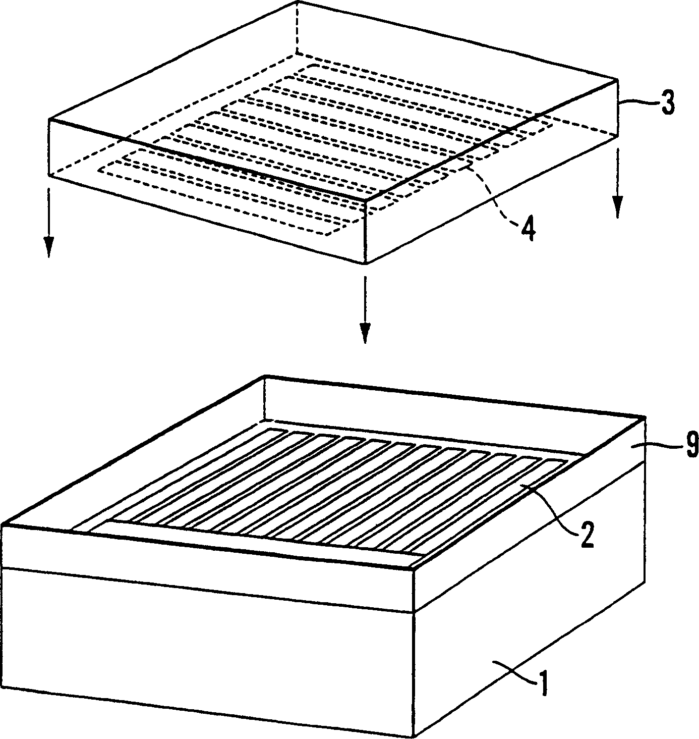
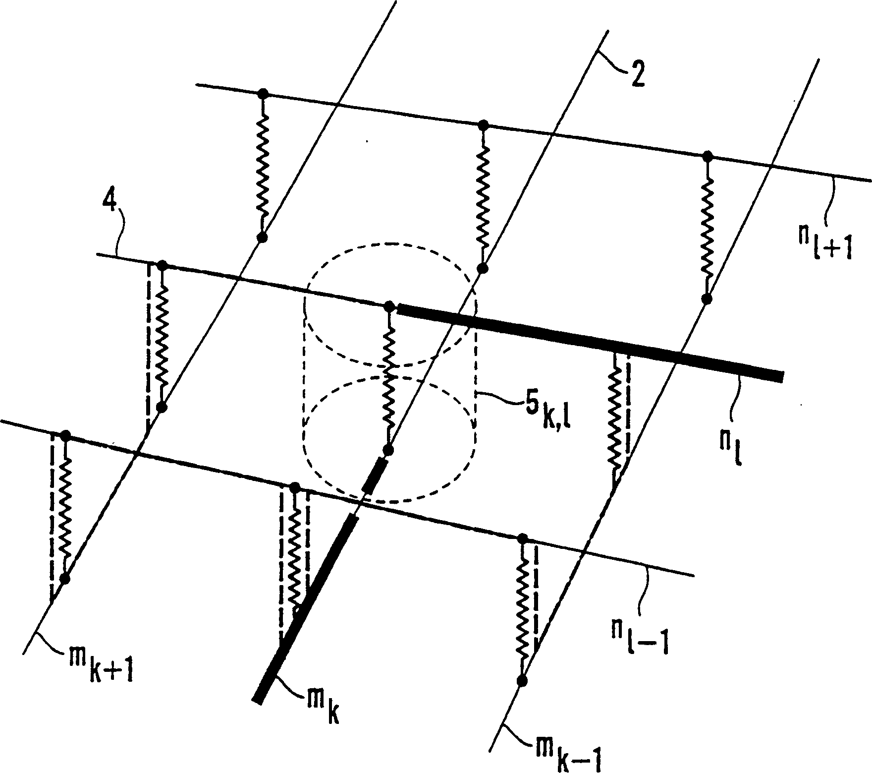
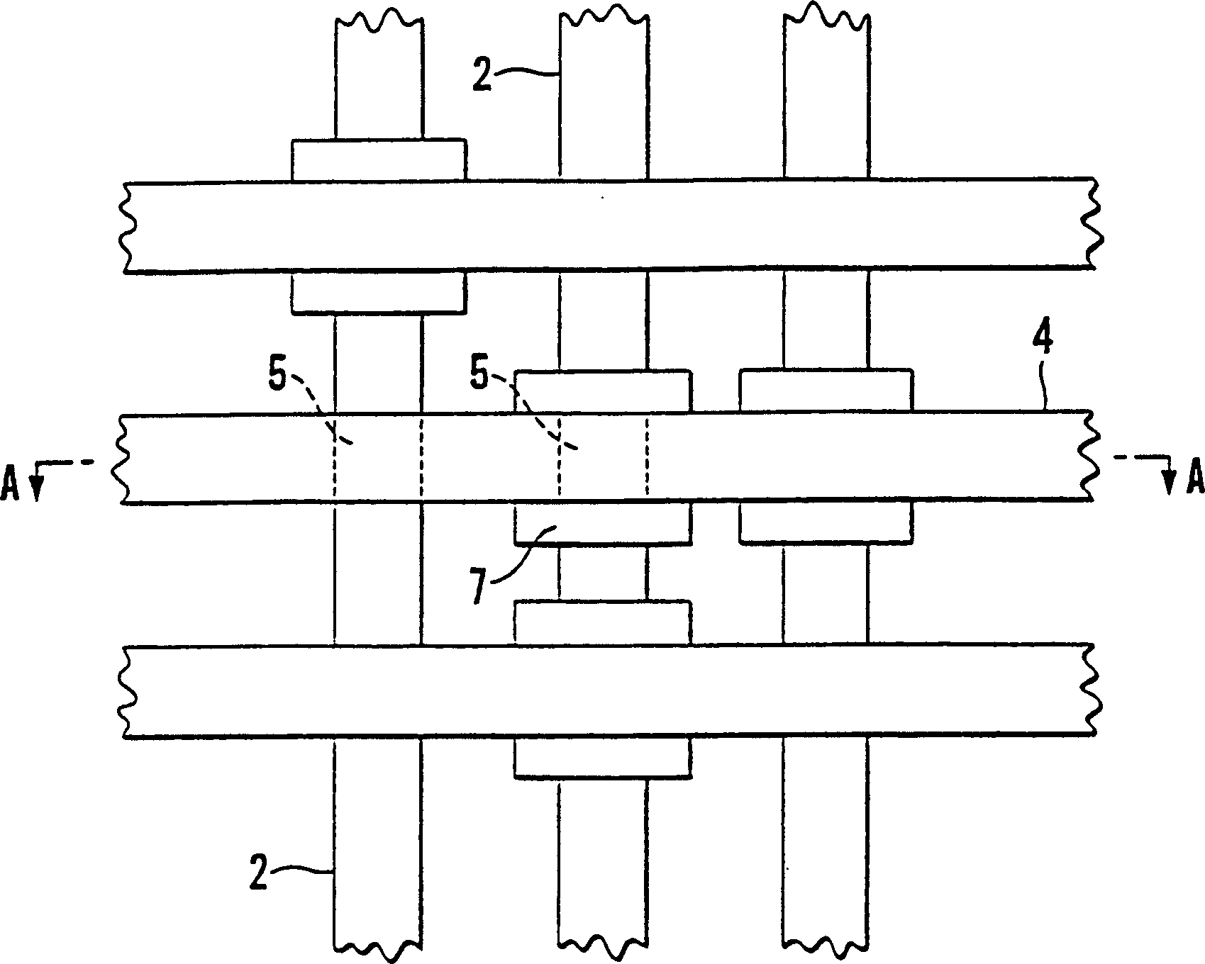
[0036] The general background of the invention is discussed in more detail below. figure 1 A general matrix addressing system is shown in , in which, for example, m wires 2 are spaced from each other and extend in the x direction, for example, n overlapping wires 4 extend in the y direction, respectively forming the first orthogonal x, y electrode matrix and a second electrode structure. The x-electrodes 2 and y-electrodes 4 are arranged relatively close to each other, thereby providing a geometrically well-defined area of ​​overlap or intersection between the two electrodes. The space around and between each intersection is roughly defined by the overlap given by the width of the intersecting x- and y-electrodes at these intersections, including those which will be denoted below as memory cells 5, see figure 2 . In the memory cell 5, the mutually overlapping area of ​​the respective x and y electrodes 2, 4 is indicated as the contact area of ​​the memory cell. According t...


PUM


Abstract

A read-only memory is made electrically addressable over a passive conductor matrix, wherein at least a portion of the volume between intersection of two conductors (2;4) in the matrix defines a memory cell (5) in the read-only memory. Data are stored as impedance values in the memory cells. The memory cells (5) comprise either an isolating material (6) which provides high impedance or one or more inorganic or organic semiconductors (9), preferably with an anisotropic conducting property. The semiconductor material (9) forms a diode junction at the interface to a metallic conductor (2;4) in the matrix. By suitable arrangement of respectively the isolating material (6) and semiconductor material (9) in the memory cells these may be given a determined impedance value which may be read electrically and corresponds to logical values in a binary or multi-valued code. The read-only memory device may be realized either as planar or also volumetrically by stacking several read-only memories (ROM) above each other and connecting them with the substrate (1) via addressing buses (14). Such read-only memory devices may be implemented on memory cards with standard card interfaces and used for storage of source information.

Description

technical field Background technique [0001] The prior art provides numerous examples of electrically addressable semiconductor read-only memories in passive matrices. U.S. Patent 4,099,260 (Lynes et al.) discloses a semiconductor read-only memory (ROM) manufactured as a large-scale integrated device, wherein self-isolated bit line surface regions of one conductivity type are formed in the semiconductor substrate directly in the opposite conductivity In the body area of ​​the type. A channel stop region of the same conductivity type as the body region is formed in the space between the bit line regions. A metallized wordline on and perpendicular to the bitline region is formed spaced from the bitline by an isolation layer. The memory cell includes a single Schottky diode. Such diodes will or will not be formed at every intersection of wordlines and bitlines, depending on whether or not openings are formed in the isolation layer during fabrication so that the wordlines make...

Claims


Application Information

Patent Timeline
IPC IPC(8): G11C16/04G11CG11C11/56G11C17/06G11C17/10H01LH01L27/02H01L27/10H01L27/102H01L27/112H01L27/28H01L51/05
CPCG11C11/5664B82Y10/00G11C11/5692H01L27/112G11C13/0016G11C13/0014H10B20/00G11C11/56
Inventor H·G·古德森P·-E·诺达尔G·I·莱斯塔德
Owner THIN FILM ELECTRONICS ASA
Why Eureka
Try Eureka