Process for preparing zero-shinkage low-temp, co-fired ceramic multi-layer baseplate
A technology of low-temperature co-fired ceramics and multi-layer substrates, which is applied in semiconductor/solid-state device manufacturing, semiconductor/solid-state device components, electrical components, etc., and can solve problems such as large plane shrinkage
- Summary
- Abstract
- Description
- Claims
- Application Information
AI Technical Summary
Problems solved by technology
Method used
Image
Examples
Embodiment 1
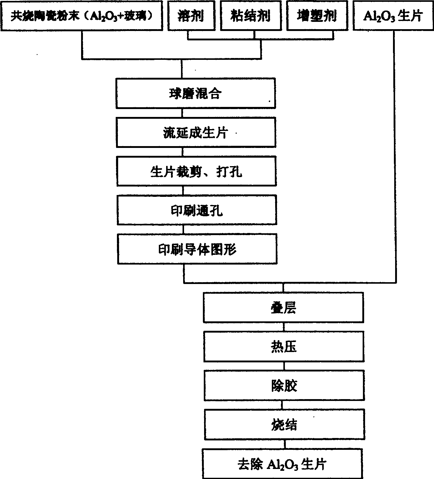
[0018] (1) Select CaO-Al 2 o 3 -B 2 o 3 -SiO 2 Glass and Al 2 o 3 Powder is made into glass ceramic powder, of which glass accounts for 55% (100.6g), Al 2 o 3 Accounting for 45% (82.0 grams), mixed with binder PVB, plasticizer DBP, solvent toluene, ball milled for 4 hours, and made into slurry;
[0019] (2) casting the slurry into a green sheet with a thickness of 125 μm, cutting it into a square, and punching;
[0020] (3) Print through holes and wiring patterns layer by layer according to the designed pattern. The through-hole conductor paste is Ag-Pd conductor paste, and the inner and outer surface patterns use Ag-Pt conductor paste;
[0021] (4) Laminate 10 green sheets sequentially, and then place an Al layer with a thickness of 0.2 mm on the bottom and top of the stack. 2 o 3 For green sheets, heat press for 1 minute at a temperature of 80°C-100°C and a pressure of 20MPa-25MPa;
[0022] (5) Continue to raise the furnace temperature to 400-450°C at a speed of ...
Embodiment 2
[0027] (1) Glass, Al 2 o 3 Raw material is identical with embodiment 1, and proportioning is different. Of which glass accounted for 45% (81.8 grams), Al 2 o 3 Accounting for 55% (100.2g), mixed with binder PVB, plasticizer DBP, solvent toluene, ball milled for 4 hours, and made into slurry;
[0028] (2) casting the slurry into a green sheet with a thickness of 125 μm, cutting it into a square, and punching;
[0029] (3) Print through holes and wiring patterns layer by layer according to the designed pattern. The through-hole conductor paste is Ag-Pd conductor paste, and the inner and outer surface patterns use Ag-Pt conductor paste;
[0030] (4) Laminate 10 green sheets in turn, and then place an Al with a thickness of 1.2 mm on the bottom and top of the stack. 2 o 3 For ceramic green sheets, keep warm for 1 minute at a temperature of 80°C-100°C and a pressure of 20MPa-25MPa;
[0031] (5) Continue to raise the furnace temperature to 400-450°C at a speed of 2°C / min, ke...
Embodiment 3
[0036] (1) Choose Na 2 O-CaO-B 2 o 3 -SiO 2 Glass and Al 2 o 3 Powder is made into glass ceramic powder, of which glass accounts for 55% (101.1g), Al 2 o 3 Account for 45% (82.3 grams), mix with binder PVB, plasticizer DBP, solvent toluene, ball mill for 4 hours, and make slurry;
[0037] (2) casting the slurry into a green sheet, cutting it into a square, and punching;
[0038] (3) Print through-holes and wiring patterns layer by layer according to the designed pattern, wherein the through-hole conductor paste is Ag-Pd conductor paste, and the inner and outer surface graphics adopt Ag-Pt conductor paste;
[0039] (4) Laminate 10 green sheets in turn, and then place an Al with a thickness of 0.5 mm on the bottom and top of the stack. 2 o 3 The green sheet is hot-pressed at a temperature of 80°C-100°C and a pressure of 15MPa for 1 minute;
[0040] (5) Continue to raise the furnace temperature to 400-450°C at a speed of 3°C / min, keep the temperature for 30 minutes, and...
PUM
| Property | Measurement | Unit |
|---|---|---|
| thickness | aaaaa | aaaaa |
| thickness | aaaaa | aaaaa |
| thickness | aaaaa | aaaaa |
Abstract
Description
Claims
Application Information


