Nitrogen gate containing silicon oxide layer structure of semiconductor device and preparation technique

A gate silicon oxide, manufacturing process technology, used in semiconductor/solid-state device manufacturing, semiconductor devices, electrical components, etc.

Inactive Publication Date: 2006-06-14
SHANGHAI INTEGRATED CIRCUIT RES & DEV CENT +1
View PDF0 Cites 0 Cited by
  • Summary
  • Abstract
  • Description
  • Claims
  • Application Information

AI Technical Summary

Problems solved by technology

The thin gate silicon oxide prepared by this method can not only effectively solve the problem of boron (B) penetration, but also enhance the reliability of the thin gate oxide layer and reduce its leakage current, and at the same time, it does not significantly affect the mobility of channel carriers. Therefore, it is an ideal thin gate silicon oxide layer that can be applied to deep submicron integrated circuits

Method used


Image

  • Nitrogen gate containing silicon oxide layer structure of semiconductor device and preparation technique
  • Nitrogen gate containing silicon oxide layer structure of semiconductor device and preparation technique

Examples


Embodiment 1

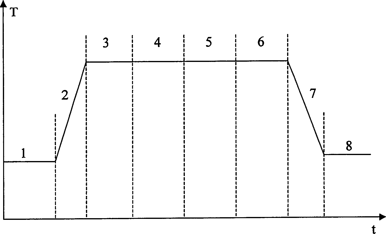
[0020] With rapid annealing oven (RTO), under normal pressure or reduced pressure

[0021] 1. In NO gas, at a temperature of 1000° C., grow a thin layer of silicon oxynitride (SiON) on the surface of a clean silicon wafer with a thickness of 8 Å.

[0022] 2. Turn off the NO gas and replace it with pure oxygen (O 2 ) gas, in this pure oxygen gas, the silicon wafer is further oxidized, that is, a thin silicon oxide (SiO) layer is grown under the newly grown SiON film, and its thickness is about 15 Å;

[0023] 3. Close O 2 Gas, then use NO gas, and anneal in this NO gas, so that a small amount of N in the NO gas diffuses to the interface between silicon oxide and silicon, forming a thin SiON interface layer with a thickness of about 3 Å;

[0024] 4. In order to further improve the quality of this gate silicon oxide, turn off the NO gas and replace it with O 2 Gas, so that the gate silicon oxide grown on it is further in O 2 Annealing in the gas for 30 seconds pushes the N ele...

Embodiment 2

[0026] 1. Using a rapid annealing furnace (RTO), under normal pressure or reduced pressure, in NO gas, at a temperature of 800°C, grow a layer of SiON on a silicon wafer with a thickness of 5 Å.

[0027] 2. Turn off the NO gas and replace it with O 2 gas to further oxidize the silicon wafer, and grow a layer of SiO under SiON with a thickness of 3 Å;

[0028] 3. Close O 2 Gas, and then replaced with NO gas, annealed in NO gas to form a SiON interface layer with a thickness of 7 Å;

[0029] 4. Turn off the NO gas and replace it with O 2 Gas, the grown gate silicon oxide will be further in O 2 Annealing in the gas for 10 seconds pushes the N element distributed on the silicon oxide-silicon interface away from the silicon surface by about 5 Å.

Embodiment 3

[0031] 1. Using a rapid annealing furnace (RTO), under normal pressure or reduced pressure, in NO gas, at a temperature of 1100°C, grow a layer of SiON on a silicon wafer with a thickness of 20 Å.

[0032] 2. Turn off the NO gas and replace it with pure oxygen gas, and grow a layer of SiO under the grown SiON film in oxygen, with a thickness of 10 Å;

[0033] 3. Close O 2 Gas, and then replaced with NO gas, annealed in NO gas, so that a small amount of NO gas diffuses to the interface between silicon oxide and silicon, forming a SiON interface layer with a thickness of 10 Å;

[0034] 4. Turn off the NO gas and replace it with O 2 or N 2 gas, making the gate silicon oxide further in O 2 or N 2 Annealing in the gas for 50 seconds pushes the N element distributed on the silicon oxide-silicon interface away from the silicon surface by about 3 Å.

[0035] The nitrogen-containing gate silicon oxide layers prepared by the above examples all have good performance, which can effec...


PUM


Abstract

The preparation process of the gate silicon oxide layer is a key process technology in the integrated circuit manufacturing process. Doping a small amount of nitrogen into conventional gate silicon oxide can improve the characteristics of gate silicon oxide. The present invention uses the rapid annealing furnace (RTO) to accurately control the characteristics of element diffusion, and uses multi-step oxidation and annealing (diffusion) methods to grow the required silicon oxide layer by layer to control the thickness of the thin gate silicon oxide layer. Thickness and distribution of nitrogen elements in the gate oxide layer. The thin gate silicon oxide prepared by this method can effectively solve the problem of boron (B) penetration, enhance the reliability of the thin gate oxide layer, and reduce its leakage current without significantly affecting the mobility of channel carriers. , so it is an ideal thin gate silicon oxide layer that can be applied to deep submicron integrated circuits.

Description

technical field [0001] The invention belongs to the technical field of integrated circuit manufacturing technology, and in particular relates to a nitrogen-containing gate silicon oxide layer structure of a semiconductor device and a manufacturing technology thereof. Background technique [0002] The preparation process of the gate silicon oxide layer is a key process technology in the integrated circuit manufacturing process, which directly affects and determines the electrical characteristics and reliability of the device, especially in the deep submicron integrated circuit manufacturing process, because the gate silicon oxide layer becomes Thinner and thinner, approaching or even working at its physical limit value, it will face many challenges, mainly in the following two aspects: (1) the electrical breakdown reliability and leakage current of thin gate silicon oxide, and the direct tunneling current problem; (2) The problem of boron penetration (Bpenetration) from P+ po...

Claims


Application Information

Patent Timeline
Patent Type & Authority Patents(China)
IPC IPC(8): H01L21/285H01L21/336H01L21/8234H01L29/78
Inventor 陈寿面
Owner SHANGHAI INTEGRATED CIRCUIT RES & DEV CENT
Why Eureka
Try Eureka