
Mask type read-only memory low heat budget making technology

A technology of read-only memory and manufacturing process, which is applied in semiconductor/solid-state device manufacturing, electrical components, circuits, etc., can solve problems such as complicated methods, increased manufacturing costs, and manufacturing process time, so as to avoid pollution, increase margins, and reduce The effect of thermal budget

Inactive Publication Date: 2006-10-11
MACRONIX INT CO LTD
View PDF0 Cites 0 Cited by
  • Summary
  • Abstract
  • Description
  • Claims
  • Application Information

AI Technical Summary

Problems solved by technology

[0004] However, although the above-mentioned "behind the gate oxide layer" manufacturing process can avoid the lateral diffusion problem caused by the thermal manufacturing process, it is much more complicated than the known method of forming the bit line first, and increases a lot of manufacturing cost and manufacturing process time

Method used


Image

  • Mask type read-only memory low heat budget making technology
  • Mask type read-only memory low heat budget making technology
  • Mask type read-only memory low heat budget making technology

Examples


Embodiment Construction

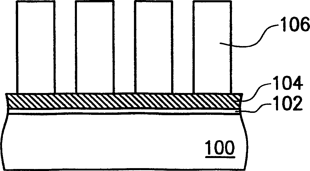
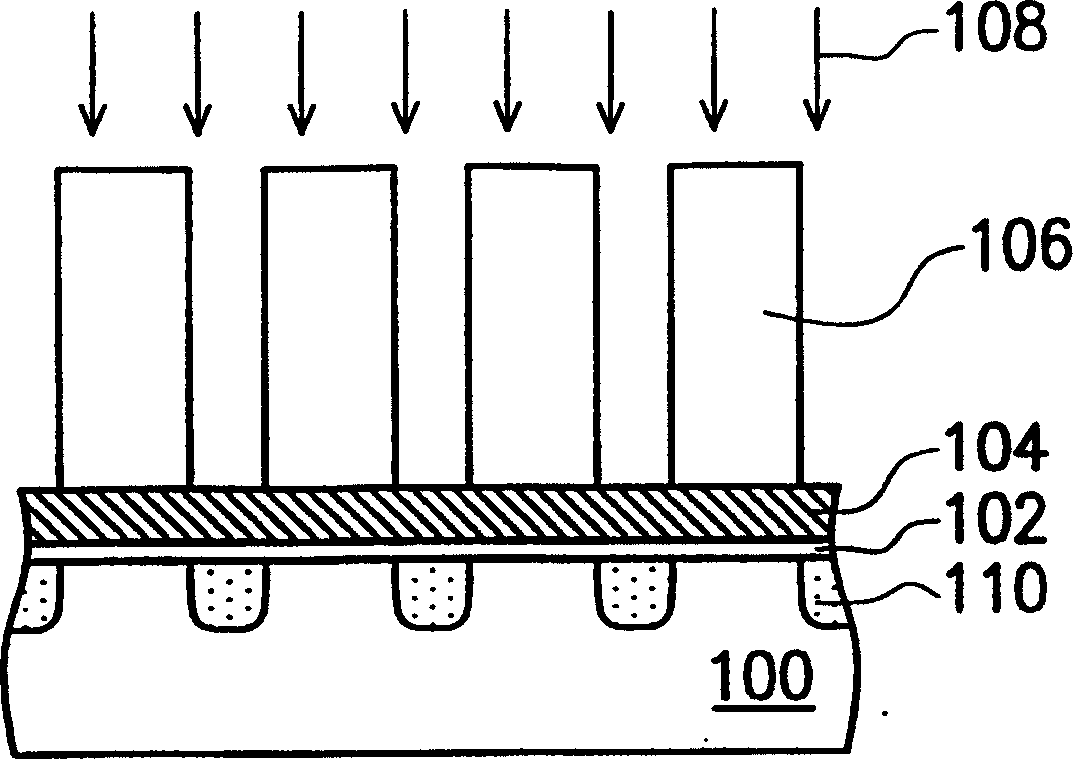
[0022] Figure 1A to Figure 1F A cross-sectional view of a manufacturing process of a mask read only memory (Mask ROM for short) low thermal budget manufacturing process according to an embodiment of the present invention.

[0023] Please refer to Figure 1A Firstly, a gate oxide layer (gate oxide) 102 is formed on a substrate 100, wherein the thickness of the gate oxide layer 102 is, for example, about 30 angstroms. Then, a first conductive layer 104 is formed on the gate oxide layer 102, the thickness of which is, for example, between 50 angstroms and 200 angstroms, and its material is, for example, polysilicon.

[0024] Then, please refer to Figure 1B , forming a first patterned photoresist layer 106 on the substrate 100 and exposing part of the first conductor layer 104 . In addition, before forming the photoresist layer 106 , a layer of bottom antireflection coating (BARC for short) may be formed on the first conductive layer 104 .

[0025] Then, please refer to Fig...


PUM


Abstract

A mask-mode read-only memory low thermal budget manufacturing process provides a substrate with a gate oxide layer on it, and then forms a first conductor layer on the gate oxide layer, and then forms several bit lines in the substrate. Next, a second conductor layer is formed on the first conductor layer, and then several read-only memory codes are formed in the substrate.

Description

technical field [0001] The present invention relates to a mask read only memory (mask read only memory, referred to as Mask ROM) manufacturing process, and in particular to a mask read only memory low thermal budget (thermal budget) manufacturing process. Background technique [0002] Mask ROM is the most basic type of ROM. In the known manufacturing process of the masked ROM, a buried bit line is formed first, and then a gate oxide, a gate layer, etc. are formed. However, the formation temperature of the gate oxide layer is generally above 800 degrees Celsius, so the dopant in the bit line often has the problem of lateral diffusion due to such a thermal process. Moreover, as the size of semiconductor devices continues to shrink, the problem of lateral diffusion caused by the above-mentioned thermal fabrication process will become more serious. [0003] Therefore, a so-called "post-gate oxide" masked ROM manufacturing process is currently proposed, which mainly forms a gat...

Claims


Application Information

Patent Timeline
Patent Type & Authority Patents(China)
IPC IPC(8): H01L21/8246H10B20/00
Inventor 黄水钦潘仁泉
Owner MACRONIX INT CO LTD
Learn More