Method for increasing crystal circlr cleaning efficiercy and improving process qualification rate

A technology of cleaning efficiency and pass rate, applied in the direction of electrical components, semiconductor/solid-state device manufacturing, circuits, etc., can solve problems such as abnormal conduction and unusable components, and achieve the goal of improving process pass rate and wafer cleaning efficiency Effect

Inactive Publication Date: 2006-10-25
MACRONIX INT CO LTD
View PDF0 Cites 1 Cited by
  • Summary
  • Abstract
  • Description
  • Claims
  • Application Information

AI Technical Summary

Problems solved by technology

For example, if the particles produced in an actual process happen to fall between the two conductive patterns of the device and cause abnormal conduction between the two conductive patterns, this will make the device unusable

Method used


Image

  • Method for increasing crystal circlr cleaning efficiercy and improving process qualification rate
  • Method for increasing crystal circlr cleaning efficiercy and improving process qualification rate
  • Method for increasing crystal circlr cleaning efficiercy and improving process qualification rate

Examples


no. 1 example

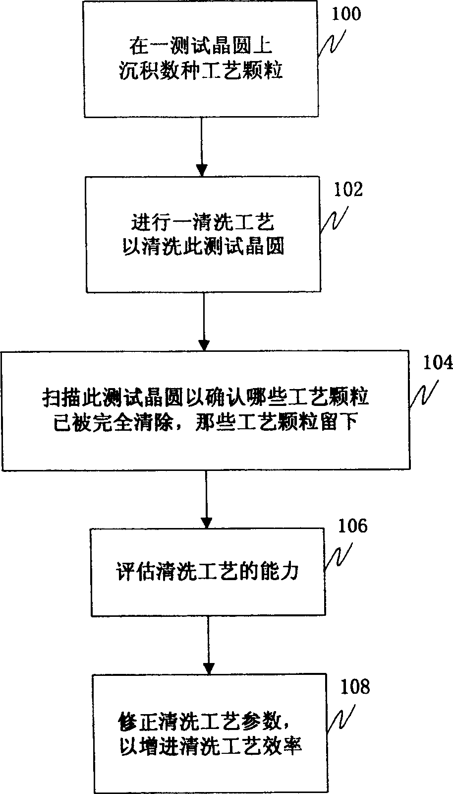
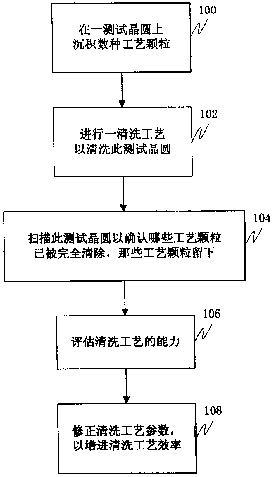
[0015] figure 1 As shown, it is a flowchart of a method for improving wafer cleaning efficiency according to a preferred embodiment of the present invention.

[0016] Please refer to figure 1 First, deposit several kinds of process particles on a test wafer (step 100). Among them, these process particles include all types of process particles in an actual process. Moreover, the process particles deposited on the test wafer further include all types of process particles of different materials, different sizes, and different shapes.

[0017] In this embodiment, the process particles deposited on the test wafer include silicon material particles, dielectric material particles, metal material particles, metal oxide particles, and so on. Among them, the silicon material particles are, for example, silicon (Si) particles and polysilicon (Polysilicon) particles. The dielectric material particles are, for example, silicon nitride (Si 3 N 4 ) Particles and silicon oxide (SiO 2 ) Particl...

no. 2 example

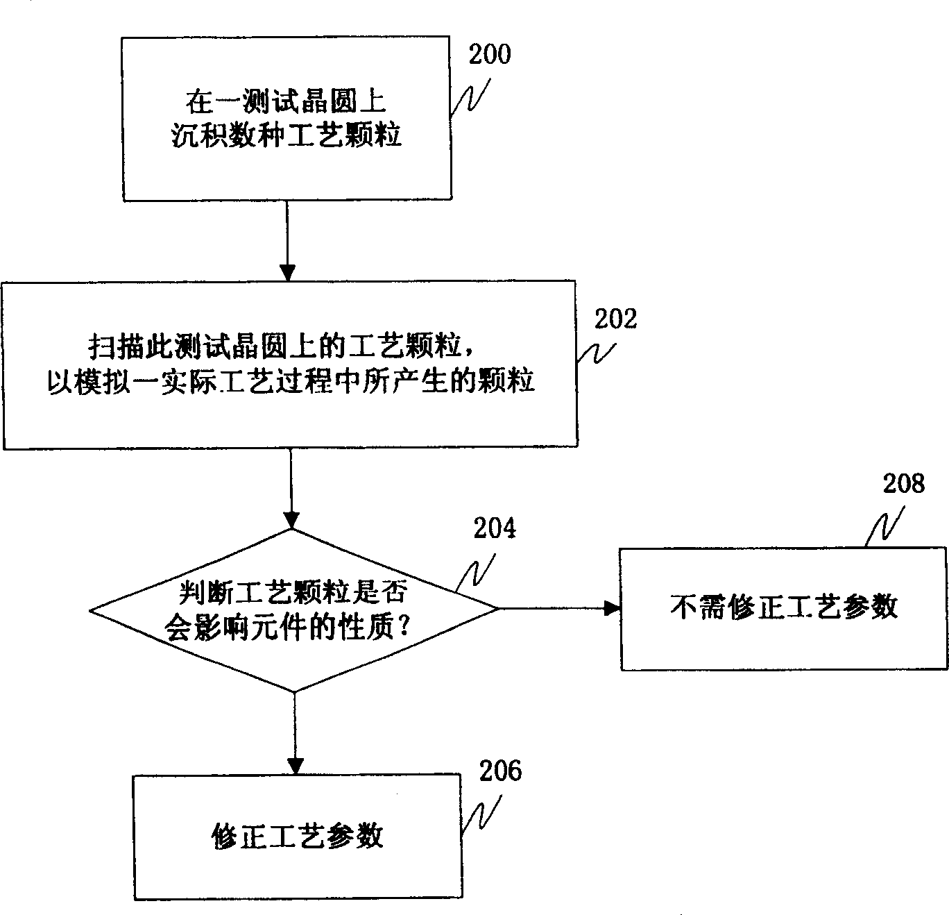
[0024] figure 2 As shown, it is a flow chart of the method for improving the process yield according to the second embodiment of the present invention.

[0025] Please refer to figure 2 First, deposit several kinds of process particles on a test wafer (step 200). Among them, these process particles include all types of process particles in an actual process. And the process particles deposited on the test wafer further include all types of process particles of different materials, different sizes, and different shapes.

[0026] In this embodiment, the process particles deposited on the test wafer include silicon material particles, dielectric material particles, metal material particles, metal oxide particles, and so on. Among them, the silicon material particles are, for example, silicon (Si) particles and polysilicon (Polysilicon) particles. The dielectric material particles are, for example, silicon nitride (Si 3 N 4 ) Particles and silicon oxide (SiO 2 ) Particles. The metal ...


PUM


Abstract

A method for improving wafer cleaning efficiency and process pass rate, wherein the method for improving wafer cleaning efficiency is to firstly deposit several kinds of process particles on a test wafer. Then a cleaning process is performed to clean the test wafer. Afterwards, the test wafer is scanned to confirm which process particles have been completely removed and which process particles remain on the test wafer. Then, a result of scanning the test wafer is used to evaluate the cleaning capability of the cleaning process. Then, modify the parameters of the cleaning process to improve the efficiency of the cleaning process.

Description

Technical field [0001] The present invention relates to a method for improving the qualification rate of a semiconductor process, and particularly relates to a method for improving the efficiency of wafer cleaning and improving the qualification rate of the process. Background technique [0002] In the integrated circuit process technology, the most frequent process step is the wafer cleaning step, which accounts for about 30% of all process steps, so its importance is naturally quite high. The main purpose of wafer cleaning is to remove impurity particles and contaminants on the surface of the wafer and reduce the adhesion of fine dust. The contamination of conductive impurity particles may cause leakage of semiconductor components, reduce component breakdown voltage, and even cause short circuits in the circuit structure, and so on. Therefore, it is very important to improve the efficiency of wafer cleaning and thus the process pass rate. [0003] In particular, during the semi...

Claims


Application Information

Patent Timeline
Patent Type & Authority Patents(China)
IPC IPC(8): H01L21/302H01L21/304H01L21/66
Inventor 马思尊张国华
Owner MACRONIX INT CO LTD
Why Eureka
Try Eureka