Method for preparing semiconductor device with super shallow and super steep backward surface groove

A surface channel, semiconductor technology, applied in semiconductor/solid-state device manufacturing, semiconductor devices, transistors, etc., can solve problems such as low productivity of doping curves and difficulty in extracting ultra-low energy ion beams

Inactive Publication Date: 2007-03-28
SK HYNIX INC
View PDF2 Cites 3 Cited by
  • Summary
  • Abstract
  • Description
  • Claims
  • Application Information

AI Technical Summary

Problems solved by technology

[0021] However, ultra-low-energy ion implantation technology is difficult to extract ultra-low-energy ion beams, and this difficulty leads to the limitation of available energy and the low productivity of establishing doping profiles of SSR surface channels

Method used


Image

  • Method for preparing semiconductor device with super shallow and super steep backward surface groove
  • Method for preparing semiconductor device with super shallow and super steep backward surface groove
  • Method for preparing semiconductor device with super shallow and super steep backward surface groove

Examples


Embodiment Construction

[0043] Other objects and aspects of the present invention will be apparent from the following description of the embodiments with reference to the accompanying drawings.

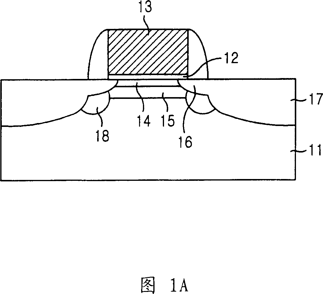
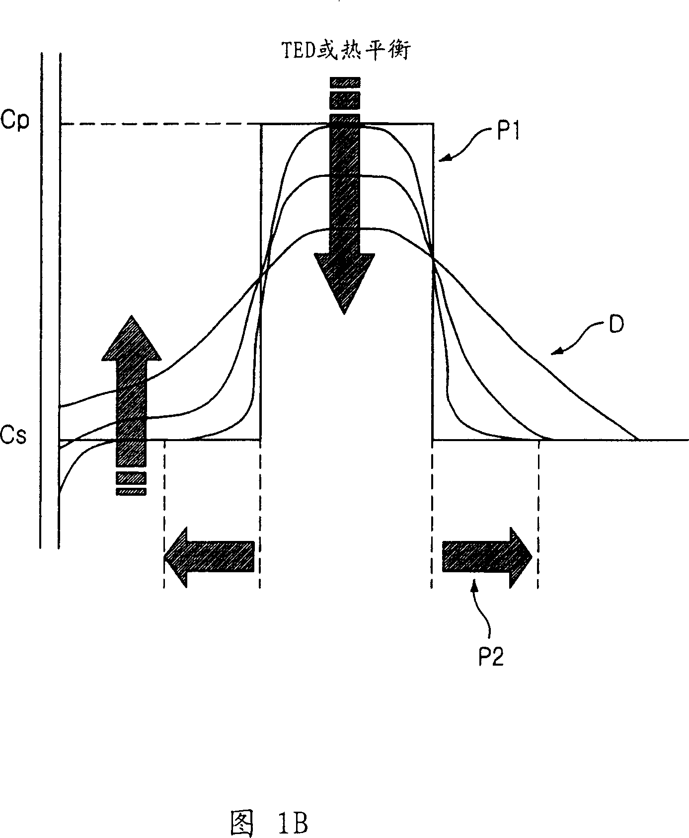
[0044] The present invention provides a method for manufacturing a semiconductor device with an ultra-shallow ultra-steep reverse (hereinafter referred to as SSR) surface channel. Compared with low-energy ion implantation technology, decaborane ion implantation technology reduces the distribution width of dopants and greatly improves productivity due to shortened process time. Therefore, this method is particularly suitable for epi-channel doping to provide ultra-shallow SSR epi-channels with improved performance and increased productivity.

[0045] Molecular formula is B 10 h 14 Decaborane is a particularly suitable source ion for implantation in the present invention. Decaborane also has a large molecular weight, capable of providing boron ions comprising 10 boron atoms when ionized. Because of these c...


PUM


Abstract

The present invention provides a method for fabricating a semiconductor device with ultra-shallow super-steep-retrograde epi-channel that is able to overcome limitedly useable energies and to enhance manufacturing productivity than using ultra low energy ion implantation technique that has disadvantage of difficulties to get the enough ion beam current as well as that of prolonged processing time. The inventive method includes the steps of: a method for fabricating a semiconductor device with ultra shallow super-steep-retrograde (hereinafter referred as to SSR) epi-channel, comprising the steps of: forming a channel doping layer below a surface of a semiconductor substrate by implanting decaborane; forming an epi-layer on the channel doping layer; forming sequentially a gate dielectric layer and a gate electrode on the epi-layer; forming source/drain extension areas shallower than the channel doping layer by being aligned at edges of the gate electrode; forming a spacers on lateral sides of the gate electrode; and forming source/drain areas deeper than the channel doping layer by being aligned at edges of the spacer through ion implantation onto the substrate.

Description

technical field [0001] The present invention relates to a kind of manufacturing method of semiconductor device; More specifically, the present invention relates to the super-steep-retrograde epi-channel (super-steep-retrograde epi-channel) with gate signal width (gate length) less than 100nm A method of manufacturing a semiconductor device. Background technique [0002] In general, in a transistor such as a metal-oxide-semiconductor field-effect transistor (MOSFET) or a metal-insulator-semiconductor field-effect transistor (MISFET), the surface region of the semiconducting substrate disposed under the gate and gate oxide functions by passing The electric field carries current, which is supplied to a source and / or drain in a state of supplying a voltage to a gate electrode. Therefore, this surface area is called a channel. [0003] The performance of the above-mentioned transistors also depends on the dopant concentration of the channel, and it is very important to dope the...

Claims


Application Information

Patent Timeline
Patent Type & Authority Patents(China)
IPC IPC(8): H01L21/336H01L27/092H01L21/265H01L21/8238H01L29/10H01L29/36H01L29/78
CPCH01L21/823807H01L29/365H01L21/26513H01L21/823892H01L29/66651H01L29/105H01L21/2658H01L21/18
Inventor 孙容宣朱晟栽
Owner SK HYNIX INC
Why Eureka
Try Eureka