Detecting method and structure for microstructure binding process

A bonding process and detection method technology, which is applied in the direction of applying stable shear force to test the strength of materials, instruments, scanning probe technology, etc., can solve the problem that the bonded sample should not be too small to reflect the bond strength , Can not accurately reflect the microstructure bonding strength and other issues, to achieve the effect of improving the processing yield of MEMS devices, convenient detection, and simple process

Inactive Publication Date: 2007-05-02
PEKING UNIV
View PDF7 Cites 0 Cited by
  • Summary
  • Abstract
  • Description
  • Claims
  • Application Information

AI Technical Summary

Problems solved by technology

[0006] The traditional detection method of sticking a small piece of bonded sample between two rigid lithographic plates and applying tension to the lithographic plates can no longer accurately reflect the strength of microstructure bonding
The reasons are: 1. The bonded sample used in the above method cannot be too small, otherwise it cannot be operated; 2. This method cannot reflect the influence of the change of the microstructure side length to area ratio and the small size effect on the bond strength.

Method used


Image

  • Detecting method and structure for microstructure binding process
  • Detecting method and structure for microstructure binding process
  • Detecting method and structure for microstructure binding process

Examples


Embodiment Construction

[0044] The present invention is mainly applicable to MEMS microstructures produced by the bonding strength detection of various microstructures using bonding techniques (for example: silicon-glass bonding, silicon ICP deep etching), and the present invention can also be used in other forms of bonding (such as silicon fusion bonding direct, adhesive bonding bonding, etc.) detection of microstructure bonding strength.

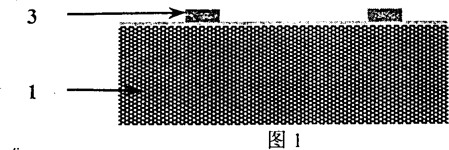
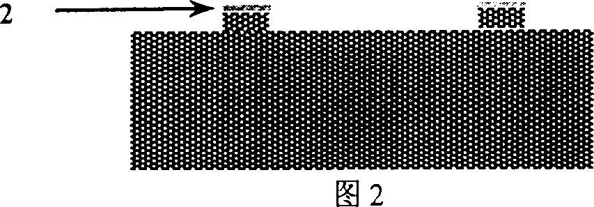
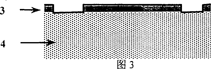
[0045] In this embodiment, the process of silicon-glass bonding and silicon ICP deep etching is specifically described, but the application of the present invention to other bonding methods is not limited. The specific process flow is shown in Figures 1-7 and their descriptions.

[0046] Silicon-glass bonding part:

[0047] In order to increase the bonding strength, necessary cleaning is performed on the bonding surfaces of the silicon structure wafer before the bonding alignment between the bonding surfaces is performed. Especially for silicon structural wafers...


PUM


Abstract

The present invention relates to detection method and detection structure for micro structure bonding process result. The detection method includes first designing silicon structure pattern; preparing micro structure with silicon structure bonded with silicon substrate or glass substrate via bonding technological process, with the silicon structure having at least one end separated from the bonding surface and the bonding area being recorded; pushing the silicon structure on the no-bonding end with micro probe to make the silicon structure deform until the monocrystal silicon chip breaks from the bonding surface and recording the distance between the probe pushed point and the bonding surface, deformation and the breaking process parameters; and calculating the bonding strength based on the recorded data. The present invention completes MEMS device detection in a simple process.

Description

Technical field: [0001] The invention relates to the technical field of micro-electro-mechanical system (MEMS) processing technology, in particular to a detection method for microstructure bonding process results and a detection structure used in the method. Background technique: [0002] As an interdisciplinary and advanced manufacturing technology that originated in the 1990s, MEMS has played an important role in improving people's quality of life, improving people's living standards and enhancing national strength. Due to the strong interdisciplinary features, MEMS research methods and processing technologies are inherently diverse. Among many processing technologies, silicon technology is gradually becoming the mainstream of MEMS technology. Bonding, as a key technology in silicon technology, has been adopted more and more in recent years. [0003] "Bulk silicon MEMS device integration method" (CN1431699) discloses a bulk silicon MEMS device integration method, and its ...

Claims


Application Information

Patent Timeline
Patent Type & Authority Patents(China)
IPC IPC(8): G01N3/24G01Q10/00
Inventor 阮勇张大成郝一龙罗葵王玮李婷贺学锋胡维王阳元
Owner PEKING UNIV
Why Eureka
Try Eureka