Booster circuit, semiconductor device, and display device

A booster circuit and semiconductor technology, which is applied in the fields of booster circuits, semiconductor devices and display devices, can solve problems such as increased current consumption, and achieve low cost and reduced manufacturing costs

Inactive Publication Date: 2007-07-25
SEIKO EPSON CORP
View PDF3 Cites 0 Cited by
  • Summary
  • Abstract
  • Description
  • Claims
  • Application Information

AI Technical Summary

Problems solved by technology

Therefore, in order to obtain the same performance as the conventional boost circuit with an external capacitor, it is necessary to increase the switching frequency of the switching element in the charge pump circuit, resulting in an increase in current consumption due to an increase in the charge and discharge current of the capacitor.

Method used


Image

  • Booster circuit, semiconductor device, and display device
  • Booster circuit, semiconductor device, and display device
  • Booster circuit, semiconductor device, and display device

Examples


Embodiment Construction

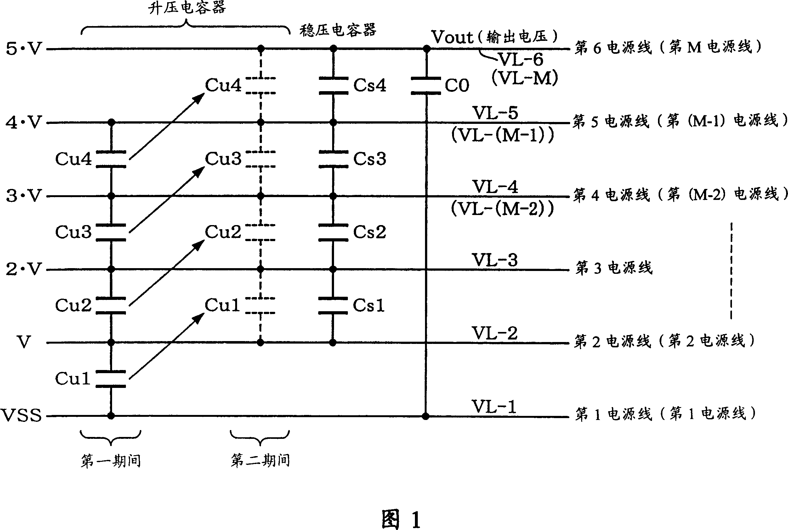
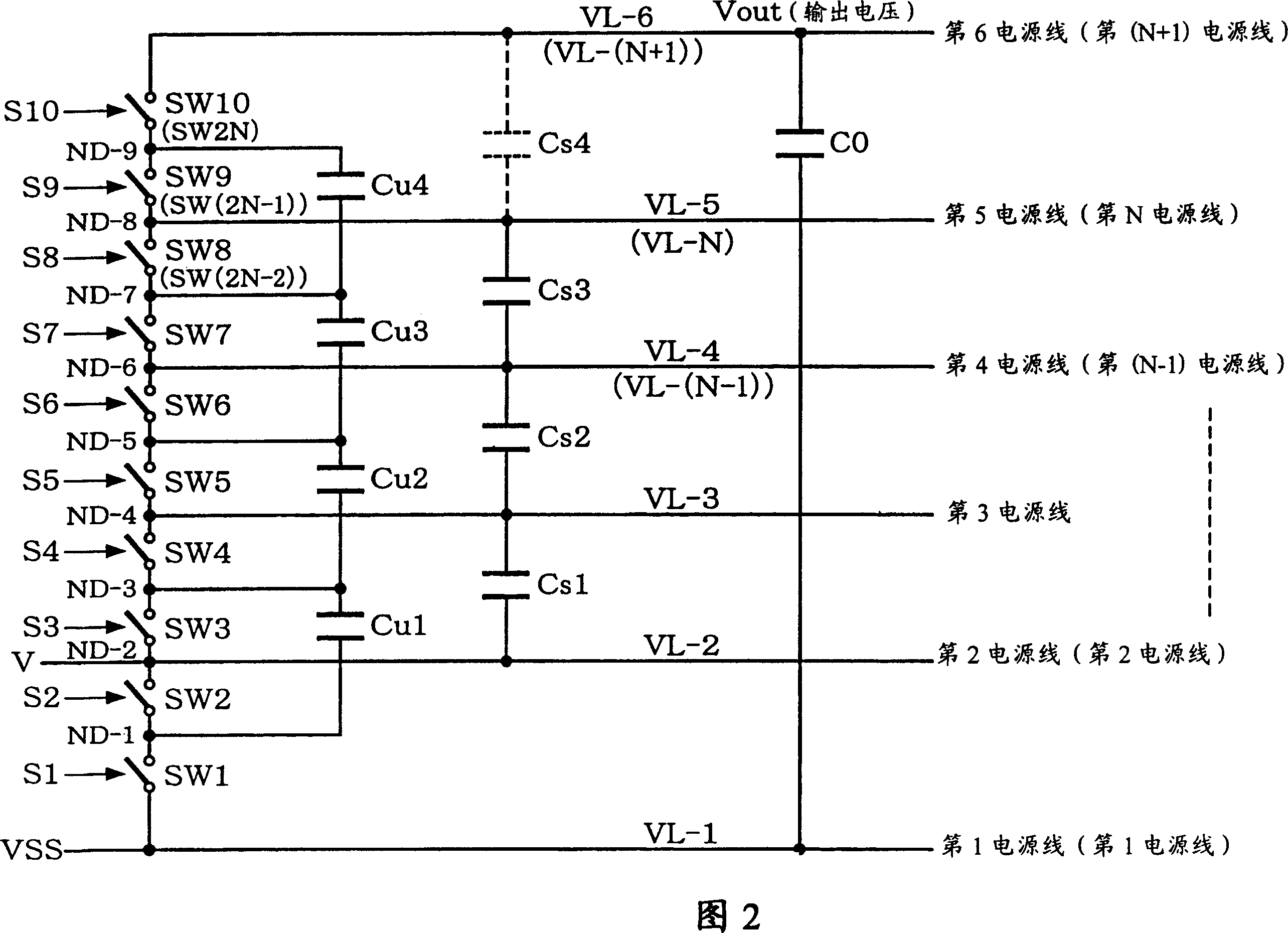
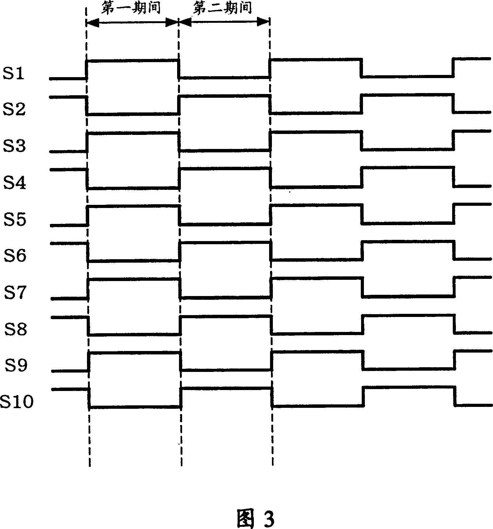
[0050] Hereinafter, preferred embodiments of the present invention will be described in detail with reference to the accompanying drawings. In addition, the embodiment described below does not unduly limit the content of the present invention described in the claims. Furthermore, not all components described below are necessarily essential components of the present invention.

[0051] 1. Boost circuit

[0052] The booster circuit of this embodiment includes a plurality of capacitors, and outputs a voltage boosted by a so-called charge pump method.

[0053] FIG. 1 is an explanatory diagram of the working principle of the boost circuit of this embodiment. The boost circuit of this embodiment includes a first power line VL- 1 to an Mth (M is an integer greater than or equal to 4) power line VL-M. In addition, the boost circuit boosts the voltage V between the first power supply line VL-1 and the second power supply line VL-2 by (M-1) times to a boosted voltage (M-1)V, and conv...


PUM


Abstract

A booster circuit includes: first to M-th power supply lines (VL-1 to VL-M) (M is an integer greater than four); first to (M-2)th boost capacitors (Cu1 to Cu(M-2)), the j-th boost capacitor (1<=j<=M-2, j is an integer) being connected between the j-th power supply line and the (j+1)th power supply line in a first period, and connected between the (j+1)th power supply line and the (j+2)th power supply line in a second period which is subsequent to the first period; and first to (M-3)th stabilization capacitors (Cs1 to Cs(M-3)), the k-th stabilization capacitor (1<=k<=M-3, k is an integer) being connected between the (k+1)th power supply line and the (k+2)th power supply line, and storing an electric charge discharged from the k-th boost capacitor in the second period.

Description

technical field [0001] The invention relates to a boost circuit, a semiconductor device and a display device. Background technique [0002] As the display device, a liquid crystal display device including an electro-optical device can be used. Mounting a liquid crystal display device in an electronic device can simultaneously achieve miniaturization and low power consumption of the electronic device. [0003] However, driving a liquid crystal display device requires a high voltage. Therefore, it is also suitable in terms of cost to incorporate a power supply circuit that generates a high voltage in a driver IC (Integrated Circuit) (semiconductor device in a broad sense) that drives an electro-optical device. At this time, the power supply circuit includes a boost circuit. The boost circuit boosts the voltage between the system power supply voltage VDD at a high potential and the ground power supply voltage VSS at a low potential to generate an output voltage Vout for driv...

Claims


Application Information

Patent Timeline
Patent Type & Authority Patents(China)
IPC IPC(8): H02M3/07H01L27/04H01L21/822
CPCH02M3/07H02M2001/009H02M1/009
Inventor 上条治雄
Owner SEIKO EPSON CORP
Why Eureka
Try Eureka