Method for manufacturing semiconductor integrated circuit device

A technology of integrated circuits and manufacturing methods, applied in the direction of semiconductor/solid-state device manufacturing, semiconductor devices, circuits, etc., can solve problems such as the inability to obtain withstand voltage

Inactive Publication Date: 2002-03-27
SANYO ELECTRIC CO LTD
View PDF0 Cites 2 Cited by
  • Summary
  • Abstract
  • Description
  • Claims
  • Application Information

AI Technical Summary

Problems solved by technology

Therefore, in the film thickness of the collector region formed of a single epitaxial layer, there is a limit in increasing the withstand voltage, and there is a problem that the required withstand voltage cannot be obtained.

Method used


Image

  • Method for manufacturing semiconductor integrated circuit device
  • Method for manufacturing semiconductor integrated circuit device
  • Method for manufacturing semiconductor integrated circuit device

Examples


Embodiment Construction

[0043] Hereinafter, embodiments of the semiconductor integrated circuit device and its manufacturing method according to the present invention will be described in detail with reference to the drawings.

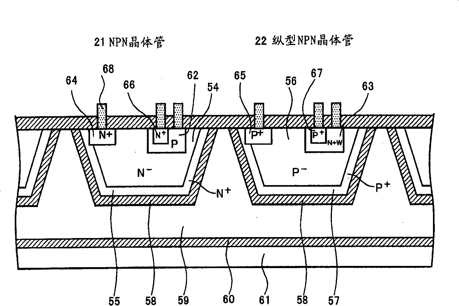
[0044] figure 1 It is a cross-sectional view of an IC of a high withstand voltage NPN transistor 21 and a high withstand voltage vertical PNP transistor 22 formed by using polysilicon 59 as dielectric isolation type complementary transistors.

[0045] In the semiconductor integrated circuit device of the present invention, polysilicon 59 is formed on support substrate 61 covered with silicon oxide film 60 . Here, the support substrate 61 and the polysilicon 59 are bonded together by performing heat treatment at 1100° C. to 1200° C. for about 2 hours through the silicon oxide film 60 . Then, a dielectric isolation type complementary type bipolar transistor is formed via the polysilicon 59 .

[0046] In the high withstand voltage NPN transistor 21, a silicon oxide film 58 an...


PUM


Abstract

The invention provides a production method for semiconductor integrated circuit device for improving the breakdown voltage of transistors in the dielectric separated complementary bipolar transistor of an NPN transistor and a longitudinal PNP transistor. In the production method for semiconductor integrated circuit device, when forming the collector area and collector extraction area of the semiconductor integrated circuit device, by laminating four epitaxial layers, the buried layer of the collector area and the buried layer of the collector extraction area are simultaneously formed for each epitaxial layer. Then, the respective buried layers are diffused, linked and etched to a V groove die. Thus, the collector area and collector extraction area made into thick films are simultaneously formed and breakdown voltage is improved.

Description

technical field [0001] The present invention relates to a semiconductor integrated circuit device and a manufacturing method thereof which realize a high withstand voltage transistor by forming a collector region thicker in a dielectric isolation type complementary bipolar transistor. Background technique [0002] In recent years, transistors used in audio amplifiers, display drivers, etc. have been required to achieve higher withstand voltage and higher integration. In order to achieve high integration and high speed of high withstand voltage integrated circuits, it is best to use dielectric isolation technology to prevent the formation of parasitic transistors or the increase in chip size caused by the formation of element isolation. [0003] exist Figure 13 A cross-sectional view of an exemplary prior art semiconductor integrated circuit device is shown in (for example, Japanese Patent Application Laid-Open No. 11-354535). Also, refer to Figure 14 ~ Figure 20 , shown ...

Claims


Application Information

Patent Timeline
Patent Type & Authority Applications(China)
IPC IPC(8): H01L29/73H01L21/304H01L21/331H01L21/76H01L21/762H01L21/8228H01L21/84H01L27/082H01L27/12
CPCH01L21/8228H01L21/84H01L21/76297H01L27/1203H01L21/76264H01L21/18
Inventor 高田忠良北村修大川重明畑博嗣藤沼近雄
Owner SANYO ELECTRIC CO LTD
Why Eureka
Try Eureka