
Defect reduction with rotated double aspect ratio trapping

An aspect ratio and high aspect ratio technology, applied in the field of semiconductor devices, can solve problems such as affecting the quality of the crystal structure of epitaxial growth

Active Publication Date: 2016-10-26
GLOBALFOUNDRIES U S INC MALTA
View PDF3 Cites 0 Cited by
  • Summary
  • Abstract
  • Description
  • Claims
  • Application Information

AI Technical Summary

Problems solved by technology

However, even with the ART procedure, a considerable number of defects may propagate to the epitaxial surface parallel to the trench direction, where these defects affect the quality of the epitaxially grown crystalline structure

Method used


Image

  • Defect reduction with rotated double aspect ratio trapping
  • Defect reduction with rotated double aspect ratio trapping
  • Defect reduction with rotated double aspect ratio trapping

Examples


Embodiment Construction

[0016] Disclosed herein are detailed embodiments of the claimed structures and methods; however, it is to be understood that the claimed structures and methods may be embodied in various forms and the disclosed embodiments are illustrative only . This invention may, however, be embodied in many different forms and should not be construed as limited to the specific embodiments illustrated herein. Rather, these illustrative embodiments are provided so that this disclosure will be thorough and complete, and will convey the scope of the invention to those skilled in the art.

[0017] In the following description, numerous specific details are provided, such as particular structures, components, materials, dimensions, processing steps and techniques, in order to provide a thorough understanding of the present invention. It will be understood, however, by one of ordinary skill in the art that the present invention may be practiced without these specific details. In other instances...


PUM


Abstract

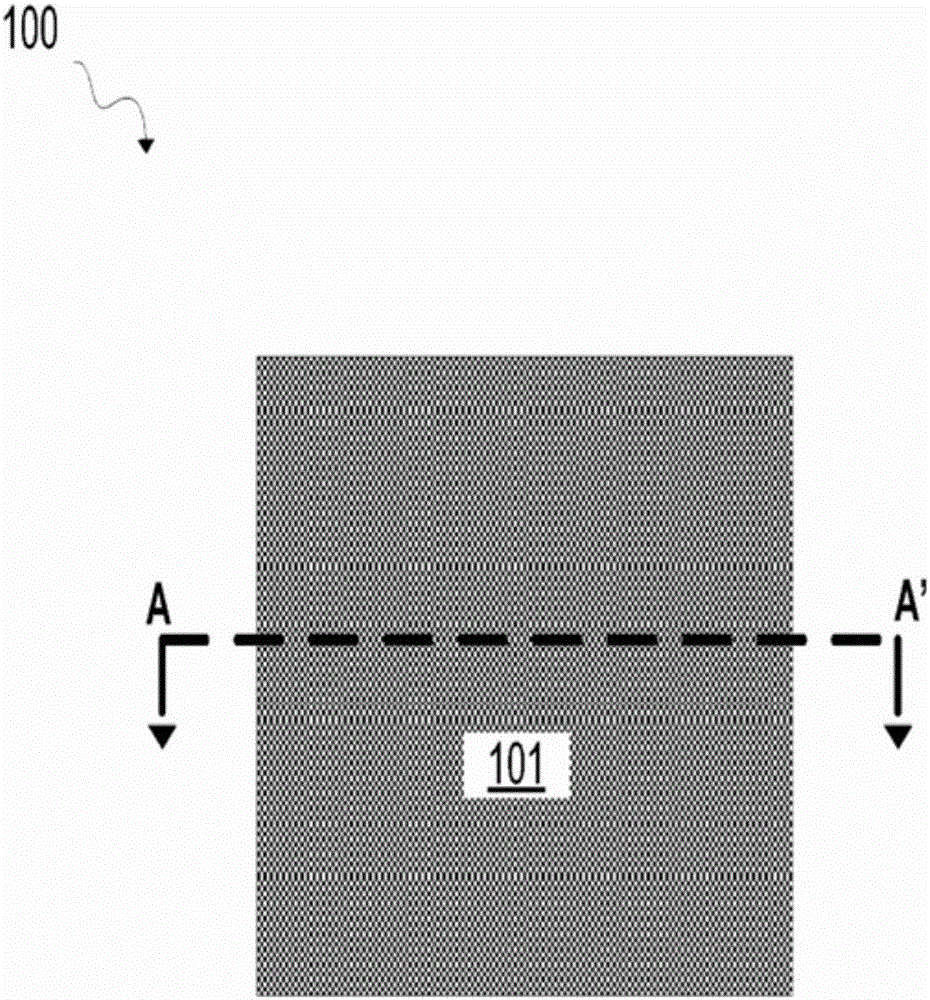
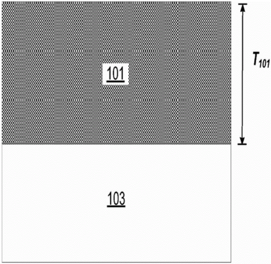
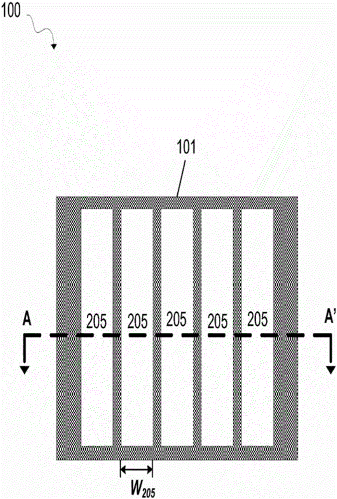
A structure and method for fabricating a heteroepitaxially grown lattice-mismatched semiconductor layer with a lower defect density is disclosed. A first semiconductor layer is epitaxially grown on an upper surface of a lattice mismatched crystalline substrate in a lower trench using a first ART deposition process. The structure is then rotated 90 degrees along a horizontal plane and a second semiconductor layer is epitaxially grown on an upper surface of the first semiconductor layer in an upper trench using a second ART deposition process. This results in an upper portion of the second semiconductor layer being substantially free of epitaxy defects.

Description

technical field [0001] Embodiments of the present invention relate generally to semiconductor devices, and more particularly to structures and methods for reducing defect density in heteroepitaxially grown materials on semiconductor substrates using a rotational dual aspect ratio trapping (ART) process. Background technique [0002] In advanced complementary metal-oxide-semiconductor (CMOS) technologies, heteroepitaxial growth of lattice-mismatched layers (i.e., germanium on silicon, III-V compounds on silicon, III-V compounds on germanium) ( heteroepitaxial growth) has practical application. However, integrating germanium or III-V compounds into conventional substrates made of silicon and / or other crystalline dielectric materials using conventional fabrication methods is challenging because of the differences in the crystalline lattice structures of the two materials. Mismatch between the two can lead to high defect formation in the resulting epitaxial structure. Lattice ...

Claims


Application Information

Patent Timeline
IPC IPC(8): H01L21/02H01L29/04H01L29/06
CPCH01L21/0242H01L21/02428H01L21/02609H01L29/045H01L29/0649H01L29/0684H01L21/02639H01L29/1054H01L29/66795H01L29/32H01L29/165H01L29/205
Inventor K·E·福格尔J·R·霍尔特P·凯尔贝A·雷兹尼切克
Owner GLOBALFOUNDRIES U S INC MALTA
Learn More