El semiconductor device

a semiconductor and light-emitting technology, applied in semiconductor devices, semiconductor lasers, lasers, etc., to achieve the effects of high reliability, excellent luminescence properties, and convenient fabrication of semiconductor light-emitting/receiving devices

Inactive Publication Date: 2009-03-05
HITACHI LTD +2
View PDF2 Cites 0 Cited by
  • Summary
  • Abstract
  • Description
  • Claims
  • Application Information

AI Technical Summary

Benefits of technology

[0025]An advantageous embodiment of the present invention provides an n-cladding layer that can be formed on an InP substrate and is suitable for optical devices such as a laser diode containing Group II-VI compound semiconductor as a main material, light emitting diode, light...

Problems solved by technology

Although inventors have used a Cl-doped MgZnCdSe or Cl-doped MgSe/Cl-doped ZnCdSe superlattice layer as a stable n-cladding la...

Method used


Image

  • El semiconductor device
  • El semiconductor device
  • El semiconductor device

Examples


Embodiment Construction

[0040]A preferred embodiment of the present invention will now be described with reference to the accompanying drawings. In the following description, same drawing reference numerals are used for the same elements even in different drawings.

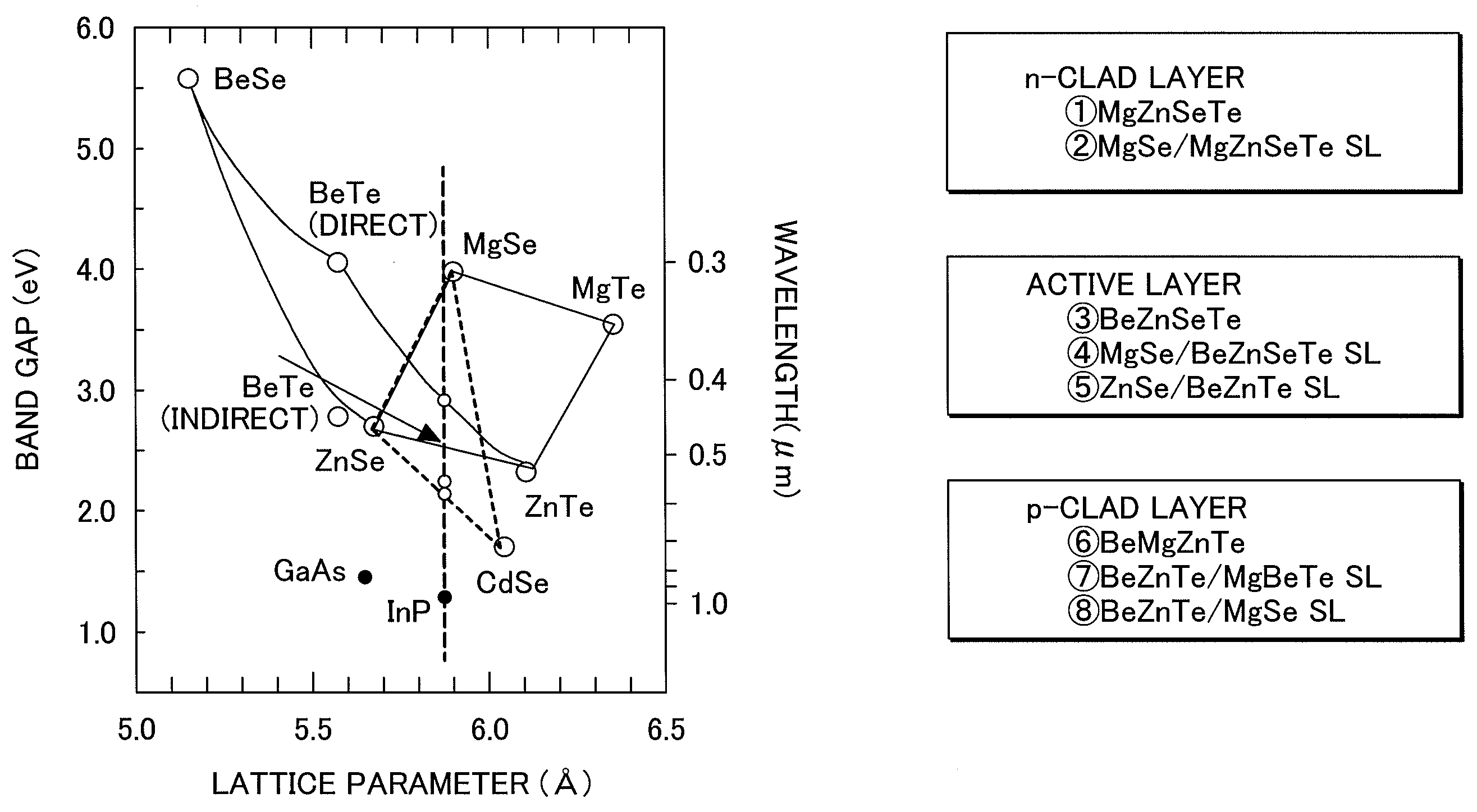
[0041]Particularly, the present invention provides the composition of a layer structure for a green semiconductor layer to be formed on an InP substrate, by utilizing a carefully selected material that satisfies the RoHS standard.

[0042]More particularly, the present invention provides a new n-cladding layer advantageous for a high concentration doping effect, an active layer suitable for the n-cladding laser according to the type of a band line-up, and a p-cladding material in relation to harmful material.

[0043]FIG. 1 illustrates a relation between lattice parameters and energy gaps of Group II-VI compound semiconductors as related to the invention. A dotted line running parallel to the vertical axis indicates a lattice parameter being lattice-ma...


PUM


Abstract

An n-type cladding layer structure which has good luminescence properties without the use of substances corresponding to RoHS Directive and a high Cl-doping efficiency, i.e. which facilitates the manufacture of a semiconductor optical element and device with low crystal defects and high reliability, and an active layer and a p-type cladding layer therefor are provided. The n-type layer being lattice matched to an InP substrate and containing Group II-VI compound as a main ingredient is a Group II-VI compound semiconductor, in which the Group II elements consist of Mg, Zn, and Be and the Group VI elements consist of Se and Te. The n-type layer of the present invention is characterized by a large energy gap, high energy of the bottom of a conduction band that is effective for suppress the Type II luminescence, high carrier concentration, and low crystal defects attributed to a good quality crystallinity.

Description

CLAIM OF PRIORITY[0001]The present application claims priority from Japanese application JP2007-225724, filed on Aug. 31, 2007, the content of which is hereby incorporated by reference into this application.BACKGROUND OF THE INVENTION[0002]1. Field of the Invention[0003]The present invention relates to an EL semiconductor device having an n-type semiconductor layer structure on an InP substrate; and, more particularly, to an EL semiconductor device, e.g., a green light emitting laser, featuring a sufficient energy gap and carrier concentration, including an n-type cladding layer made out of II and VI group elements and capable of trapping and confining light and carriers.[0004]2. Background of the Related Arts[0005]An EL semiconductor device, e.g., a semiconductor laser diode (LD), is a light source used for recording or reproducing data onto or from an optical disc. Historically, most of the research has been focused on development of a light source with a shorter wavelength to be ...

Claims


Application Information

Patent Timeline
IPC IPC(8): H01S5/32H01L33/06H01L33/28H01L33/30
CPCH01S5/0218H01S5/0421H01S5/327H01S5/3059H01S5/305
Inventor KISHINO, KATSUMINOMURA, ICHIROASATSUMA, TSUNENORITASAI, KUNIHIKOTAMAMURA, KOSHINAKAJIMA, HIROSHINAKAMURA, HITOSHIFUJISAKI, SUMIKOKIKAWA, TAKESHI
Owner HITACHI LTD
Why Eureka
Try Eureka