Semiconductor memory device and memory modulus and system adopting same

A technology of storage device and storage module, which is applied in the direction of memory system, static memory, digital memory information, etc.

Inactive Publication Date: 2010-05-05
SAMSUNG ELECTRONICS CO LTD
View PDF2 Cites 0 Cited by
  • Summary
  • Abstract
  • Description
  • Claims
  • Application Information

AI Technical Summary

Problems solved by technology

Likewise, the operating characteristics of register 108 may limit the effective operating speed of the memory to less than the system clock speed

Method used


Image

  • Semiconductor memory device and memory modulus and system adopting same
  • Semiconductor memory device and memory modulus and system adopting same
  • Semiconductor memory device and memory modulus and system adopting same

Examples


Embodiment Construction

[0034] Preferred embodiments of the present invention will now be described in detail with reference to the accompanying drawings, wherein like elements are designated by like numerals.

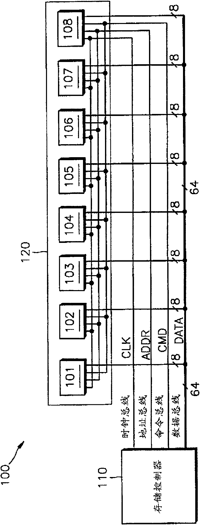
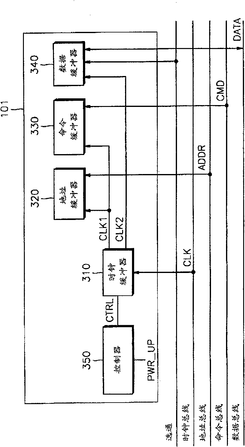
[0035] image 3 A semiconductor memory device of a first embodiment of the present invention is explained. The semiconductor memory device 101 generally corresponds to a memory module (such as figure 1 One of the memory chips included in the module 120 ) includes a clock buffer 310 , an address buffer 320 , a command buffer 330 , a data buffer 340 and a controller 350 . The clock buffer 310 receives the clock signal CLK on the clock bus (herein referred to as "external clock signal"), and generates internal clock signals CLK1 and CLK2. Relative frequencies of the first internal clock signal CLK1 and the second clock signal CLK2 are determined by the clock buffer 310 in response to the control signal CTRL output from the controller 350 . For example, the control signal CTRL may specify whet...


PUM


Abstract

A semiconductor memory device includes a clock buffer which receives an external clock signal and generates a first internal clock signal having a frequency lower than that of the external clock signal and a second internal clock signal having a frequency which is the same as that of the external clock signal. An address buffer, command signal buffer and / or register receive respective input signals at a timing of the first internal clock signal. On the other hand, a data buffer inputs / outputs data at a timing of the second internal clock signal.

Description

technical field [0001] The invention relates to a memory device, a memory module and a system, in particular to a semiconductor memory device generating an internal clock signal and a memory module and a system using the semiconductor memory device. Background technique [0002] The growing need for computer systems capable of processing large amounts of data at high speeds has led to the continued development of efficient microprocessors or central processing units (CPUs), which tend to run at higher and higher system clock frequencies. One of the requirements for the use of a higher system clock frequency is an increase in the data capacity and transfer speed of the data memory interfaced with the CPU. In other words, the memory must be configured to run synchronously with the higher frequency system clock signal. [0003] figure 1 is a diagram of the memory controller 110 and the memory module 120 of the CPU system board 100 . The storage controller 110 transmits a clo...

Claims


Application Information

Patent Timeline
Patent Type & Authority Patents(China)
IPC IPC(8): G11C11/34G11C11/407G06F12/00G06F12/06G06F13/16G11C7/10G11C7/22G11C8/18G11C11/401G11C11/4076G11C11/408G11C11/4093
CPCG11C11/4082G11C7/1072G11C8/18G11C7/109G11C7/222G11C7/1084G11C7/1078G11C7/22G11C11/4093G11C11/4076
Inventor 李东阳
Owner SAMSUNG ELECTRONICS CO LTD
Why Eureka
Try Eureka