Crystal covered package substrate

A technology of assembly and substrate, applied in the direction of electrical components, electric solid devices, circuits, etc., can solve the problems of long current path, large plane inductance value, large inductance value variation, etc.

Inactive Publication Date: 2002-12-25
VIA TECH INC
View PDF0 Cites 4 Cited by
  • Summary
  • Abstract
  • Description
  • Claims
  • Application Information

AI Technical Summary

Problems solved by technology

However, the signal solder ball pads 136a, the power solder ball pads 136b and the ground solder ball pads 136c of the known flip-chip package substrate 130 are all irregularly distributed on the bottom surface 134 of the flip-chip package substrate 130, which does not correspond to meets the Figure 2A The internal and ex

Method used


Image

  • Crystal covered package substrate
  • Crystal covered package substrate
  • Crystal covered package substrate

Examples


Embodiment Construction

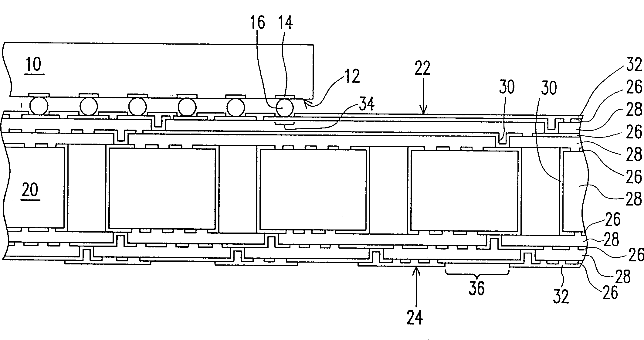
[0057] Please refer to figure 1 , Figure 4 ,in Figure 4 It is a partial top view of a flip-chip substrate of a preferred embodiment of the present invention. Figure 4 The composition structure of the flip-chip substrate 200 is the same as figure 1 The composition structure of the flip-chip substrate 20 includes a multi-layer patterned wiring layer 26, at least one insulating layer 28 and a plurality of conductive plugs 30, wherein these wiring layers 26 overlap each other in sequence, and the insulating layer 28 is They are respectively arranged between two adjacent wire layers 26 to isolate the wire layers 26 and overlap with the wire layers 26. The conductive plugs 30 respectively penetrate through the insulating layer 28 to electrically connect the wire layers 26. . also, figure 1 The top surface 22 and the bottom surface 24 of the flip-chip substrate 20 also have a solder mask layer 32 to protect the outermost conductive layer 26 and the underlying insulating layer...


PUM


Abstract

A crystal covered packaging substrate is composed of the multilayer patternized wire layer in at least one insulation layer and at least one conductive plug of which the wire layer is overlapped to each other in sequence, the insulation layer is configurated in between the two adjacent wire layers and the conductive plug is running through the insulation layer to connect the wire layers electrically. There are several lug pads at top layer of the wire layers and there are several welding ball pads at bottom layer of the wire layers. In addition, there are multicircles of lug pad rings formed by lug pads at the top face of the crystal covered packaging substrate and multicircules of welding ball pad rings formed by welding ball pads corresponded to the lug pad ring at the bottom face of which the internal-external relative positions of lug pad rings.

Description

technical field [0001] The present invention relates to a flip-chip substrate, and in particular to a flip-chip substrate capable of reducing planar inductance effects and synchronous switching noise (Synchronous Switching Noise, SSN). Background technique [0002] Flip Chip technology (Flip Chip, FC) is a packaging technology often used in Chip Scale Package (CSP). Die pads are arranged on the active surface of the chip, and bumps are formed on each pad, and then the bumps on the chip are connected to the contacts of the carrier (carrier) correspondingly. contact), the so-called bump pad. Since the flip-chip bonding technology has the advantages of reducing the packaging area and shortening the signal transmission path, the flip-chip bonding technology has been widely used in the field of chip packaging. [0003] Please refer to figure 1 , which is a cross-sectional view of a known flip-chip structure. The flip-chip substrate 20 is mainly composed of multi-layer pattern...

Claims


Application Information

Patent Timeline
IPC IPC(8): H01L23/14
Inventor 许志行徐鑫洲
Owner VIA TECH INC
Why Eureka
Try Eureka