Interconnection device for a printed circuit board, a method of manufacturing the same, and an interconnection assembly having the same

a technology of printed circuit boards and interconnection devices, which is applied in the manufacture of contact parts, coupling device connections, instruments, etc., and can solve the problems of difficult assembly process, high processing cost, and loss of processing tim

Active Publication Date: 2006-07-27
PHICOM CORP +1
View PDF19 Cites 24 Cited by
  • Summary
  • Abstract
  • Description
  • Claims
  • Application Information

AI Technical Summary

Benefits of technology

[0014] Accordingly, an object of the present invention is to provide an interconnect device for a printed circuit board, a method of manufacturing the same, and an interconnect assembly having the same which are capable of omitting the wire bonding process for attaching the resilient contact elements such as springs to the substrate so as to solve related problems such as difficulties in the manufacturing processes caused by the bonding process.

Problems solved by technology

Therefore, a process of fabricating the assembly is very difficult and causes a lot of processing time losses.
This makes the process more difficult and causes more processing time losses.
Along with the above problems, since the resilient contact elements such as springs are attached to both top and bottom surfaces of the substrate 302 by the wire bonding process or the like, the attached portions can be easily deteriorated.
In addition, since the resilient contact elements such as springs are attached to both top and bottom surfaces of the substrate, the total path length of the electrical signal increases so that electrical noises can easily occur.
In addition, since the probe card assembly comprises an element, the interposer which includes the substrate, the total cost of manufacturing the probe card assembly increases.

Method used


Image

  • Interconnection device for a printed circuit board, a method of manufacturing the same, and an interconnection assembly having the same
  • Interconnection device for a printed circuit board, a method of manufacturing the same, and an interconnection assembly having the same
  • Interconnection device for a printed circuit board, a method of manufacturing the same, and an interconnection assembly having the same

Examples


Embodiment Construction

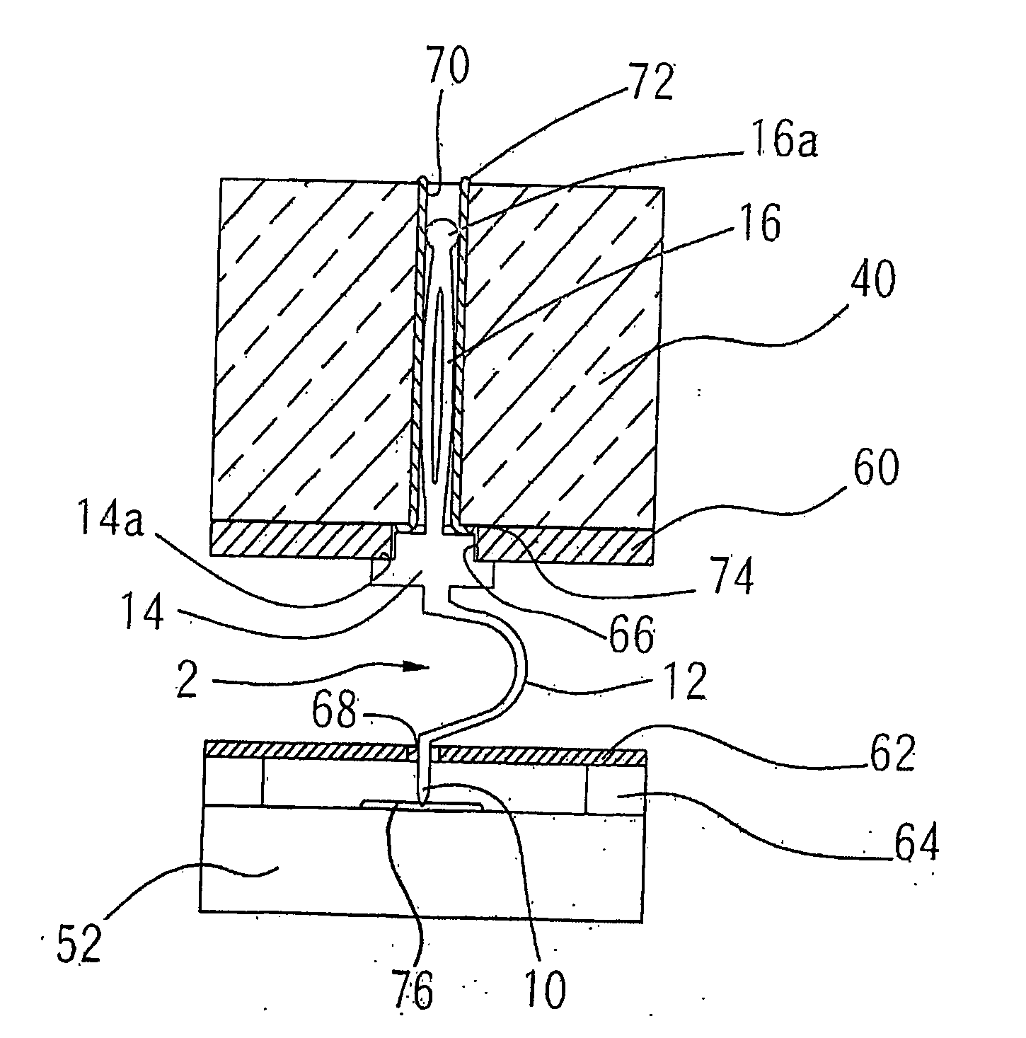
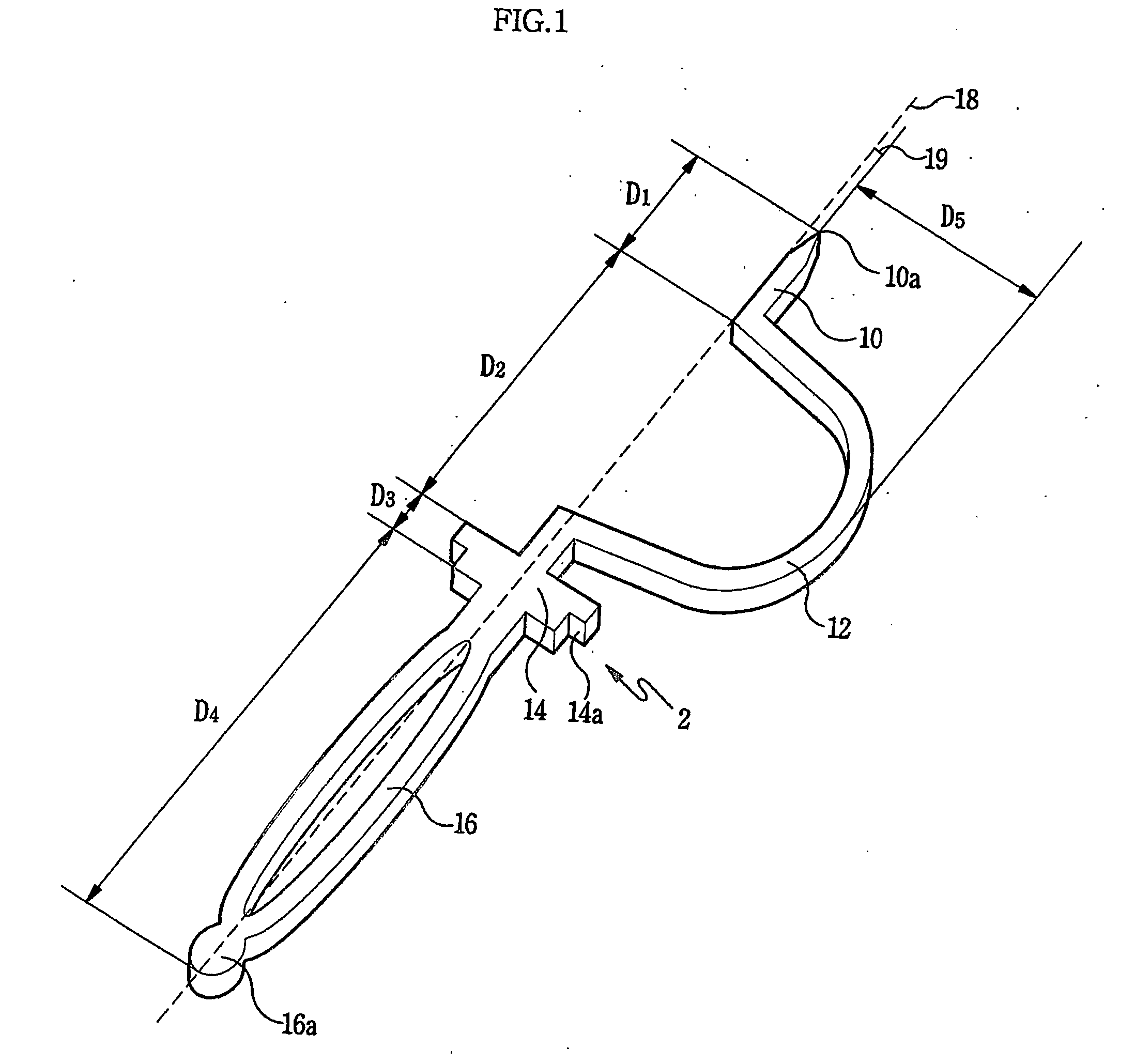
[0026] In order to achieve the above objects, the interconnect device 2 for a printed circuit board according to one aspect of the present invention comprises: a first contact section 10 having a bar-like shape for making contact with a second contact terminal 76 in a space transformer 52; a connecting section 12 having an O-ring-like shape of which one side is opened and connected to one end of the first contact section 10 in an integrated manner; a support section 14 having an engaging protrusion 14a in a predetermined portion and connected to one end of the connecting section 12 in an integrated manner; and a second contact section 16 having an O-ring-like shape and connected to one end of the support section 14 in an integrated manner, wherein the whole interconnect device is made up of an identical resilient material.

[0027] Now, each element of the interconnect device 2 will be described in detail with reference to the accompanying drawings.

[0028] First, the interconnect devi...


PUM

PropertyMeasurementUnit
total length D1aaaaaaaaaa
total length D2aaaaaaaaaa
total length D5aaaaaaaaaa

Abstract

The present invention relates to an interconnect device for a printed circuit board, a method of manufacturing the same and an inter-connect assembly having the same. According to one aspect of the present invention, the interconnect device for a printed circuit board comprises: a first contact section 10 having a bar-like shape for making contact with a second contact terminal 76 in a space transformer 52; a connecting section 12 having an O-ring-like shape of which one side is opened and connected to one end of the first contact section 10 in an integrated manner; a support section 14 having an engaging protrusion 14a in a predetermined portion and connected to one end of the connecting section 12 in an integrated manner; and a second contact section 16 having an O-ring-like shape and connected to one end of the support section 14, wherein the whole inter-connect device is made up of an identical resilient material. According to still another aspect of the present invention, an interconnect assembly having an interconnect device for a printed circuit board, comprises: a printed circuit board 40 including a contact hole 70 in which a conductive film 72 connected to an internal circuitry is formed on the inside wall; a first guide film 60 fixed on a bottom surface of the printed circuit board 40 and having a first guide opening 66 to open the contact hole 70; a space transformer having a second contact terminal 76 on a top portion and a bump 64 in the vicinity of the second contact terminal 76; a second guide film 62 fixed on the space transformer 52, supported by the bump 64, and having a second guide opening 68 to be related with the bump 64; and an interconnect device 2 including a second contact section having an O-ring-like shape to be inserted into the contact hole 70 by an interference fit, a support section connected to the second contact section in an integrated manner to be inserted into the inside of the first guide opening, a connecting section having an O-ring-like shape of which one side is opened and connected to the support section in an integrated manner thereby being placed between the first guide film and the second guide film, and a first contact section connected to the connecting section in an integrated manner for making contact with the second contact section 76 through the second guide opening.

Description

FIELD OF THE INVENTION [0001] The present invention relates to an interconnect device for a printed circuit board, a method of manufacturing the same, and an interconnect assembly having the same, and more specifically to an interconnect device for a printed circuit board which holds resilient forces as well as electrically interconnects an upper substrate with a lower substrate, a method of manufacturing the same and an interconnect assembly having the same. BACKGROUND OF THE INVENTION [0002] Typically, a semiconductor device is implemented on a wafer by repeating wafer processes such as an oxidation process, a diffusion process, an etching process, and a metallization process, and then slicing and packaging processes are performed to make a shipment. In addition, the semiconductor device implemented on the wafer is subject to a probing test for verifying whether it is acceptable or not after completing the wafer processes but before slicing them. [0003] In such a probing test, pre...

Claims


Application Information

Patent Timeline
Patent Type & Authority Applications(United States)
IPC IPC(8): H01L21/4763H01L23/48H01L23/52H01L29/40H01R13/05G01R31/28H01R12/04H01R12/58H01R13/24H01R43/16
CPCG01R1/06716Y10T29/49204H01R12/585H01R13/2435H01R43/16H01R2201/20H01R12/714H01L2924/00013G01R31/2889G01R1/06733H01L2924/0002H01L2224/29099H01L2924/00H01R13/05
Inventor SEO, DONGWEONHWANG, JUNTAE
Owner PHICOM CORP
Why Eureka
Try Eureka