Organic luminescent device containing coloured neutral dopant in hole transfer layer and/or electronic transfer layer

A technology of organic light-emitting devices and hole transfer, which is applied in the fields of electric solid-state devices, electroluminescent light sources, semiconductor/solid-state device manufacturing, etc., which can solve the problems of changing the electroluminescent color of devices, and achieve high luminous efficiency and long operating life , the effect of excellent brightness performance

Inactive Publication Date: 2003-01-08
GLOBAL OLED TECH
View PDF11 Cites 5 Cited by
  • Summary
  • Abstract
  • Description
  • Claims
  • Application Information

AI Technical Summary

Problems solved by technology

The problem with this scheme is that some dopants, such as rubrene, change the electroluminescence color of the device

Method used


Image

  • Organic luminescent device containing coloured neutral dopant in hole transfer layer and/or electronic transfer layer
  • Organic luminescent device containing coloured neutral dopant in hole transfer layer and/or electronic transfer layer
  • Organic luminescent device containing coloured neutral dopant in hole transfer layer and/or electronic transfer layer

Examples


Embodiment 2

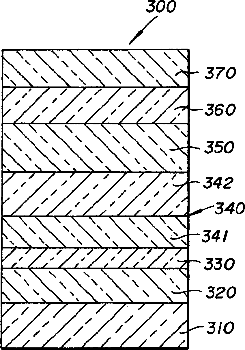
[0075] use as image 3 The structure shown, constructs the OLED of the present invention. The hole transport layer (340) consists of a 120nm undoped NPB sublayer (341) and a 30nm NPB sublayer (342) doped with ADN as a color-neutral dopant, ADN accounting for 5% of the sublayer . In all other respects, the structure and construction of this device was the same as that of the OLED of Comparative Example 1. The initial luminous efficiency, CIE coordinate value, and driving voltage are also shown in Table I. The relative luminance and drive voltage as a function of operating time are also shown in Image 6 with 7 middle. Example 3

Embodiment 3

[0076] use as Figure 4 The structure shown, constructs the OLED of the present invention. The electron transport layer (460) consists of a 20nm Alq sublayer (461) doped with ADN as a color-neutral dopant, ADN accounting for 5% of the layer, and a 15nm undoped Alq sublayer (462) . In all other respects, the structure and construction of this device was the same as that of the OLED of Comparative Example 1. The initial luminous efficiency, CIE coordinate value, and driving voltage are also shown in Table I. The relative luminance and drive voltage as a function of operating time are also shown in Image 6 with 7 middle. Example 4

Embodiment 4

[0077] use as Figure 5 The structure shown, constructs the OLED of the present invention. The hole transport layer (540) consists of a 120nm undoped NPB sublayer (541) and a 30nm NPB sublayer (542) doped with ADN as a color-neutral dopant, ADN accounting for 5% of the sublayer . The electron transport layer (560) consists of a 20nm Alq sublayer (561) doped with ADN as a color-neutral dopant, ADN accounting for 5% of the layer, and a 15nm undoped Alq sublayer (562) . In all other respects, the structure and construction of this device was the same as that of the OLED of Comparative Example 1. The initial luminous efficiency, CIE coordinate value, and driving voltage are also shown in Table I. The relative luminance and drive voltage as a function of operating time are also shown in Image 6 with 7 middle.

[0078] Example

[0079] exist Image 6 with 7 In , the stitch corresponding to the corresponding embodiment is identified by the number to the right of t...


PUM

PropertyMeasurementUnit
Thicknessaaaaaaaaaa

Abstract

The invention relates to the method for polycrystal agglutinating luminous element with high productivity. The multiple luminous elements are placed on the loading board with aid of the flexible diaphragm, which provides proper pressing force. Thus, the multiple luminous elements, the loading board and the nonistropic conducting resin layer are closely glued. The heating element can be embedded into the diaphragm. With the luminous element being pressed, the heating element heats the conducting resin, making the conducting resin solidify so as to realize the permanent mechanical and electrical connection between the luminous elements and the loading board.

Description

technical field [0001] The present invention relates to organic electroluminescent devices, and more particularly to doping hole transport layers and / or electron transport layers with suitable color-neutral dopants to improve the operating lifetime of these devices without affecting the electroluminescence color. Background technique [0002] Organic electroluminescent devices (OLEDs) in conventional form comprise a substrate and a multilayer structure located thereon, the multilayer structure comprising an anode, an optional hole injection layer, a hole transport layer, an emissive layer, an optional electron transport layer layers, and cathodes, each layer of the multilayer structure includes one or more organic or organometallic compounds. Electroluminescent (EL) devices are attractive because of their low drive voltage, high brightness, wide viewing angle, and ability to be used in full-color flat-panel emitting displays. Such OLED structures are described by Tang and ...

Claims


Application Information

Patent Timeline
IPC IPC(8): H05B33/26C09K11/06H01L51/00H01L51/30H01L51/50
CPCH01L51/005Y10S428/917H01L51/0065H01L51/0058H01L51/5012Y10T428/26H10K85/60H10K85/653H10K85/626H10K50/11H05B33/26
Inventor T·K·哈特瓦尔R·H·杨
Owner GLOBAL OLED TECH
Why Eureka
Try Eureka