

Base board transporting device, base board processing system and base board transporting method
A substrate processing system and substrate handling technology, applied in thin material processing, transportation and packaging, optics, etc., can solve the problems of high device cost, inability to detect position offset, time waste, etc.
- Summary
- Abstract
- Description
- Claims
- Application Information
AI Technical Summary
Problems solved by technology
Method used
Image

Examples
Embodiment Construction
[0040] Hereinafter, embodiments of the present invention will be described based on the drawings.
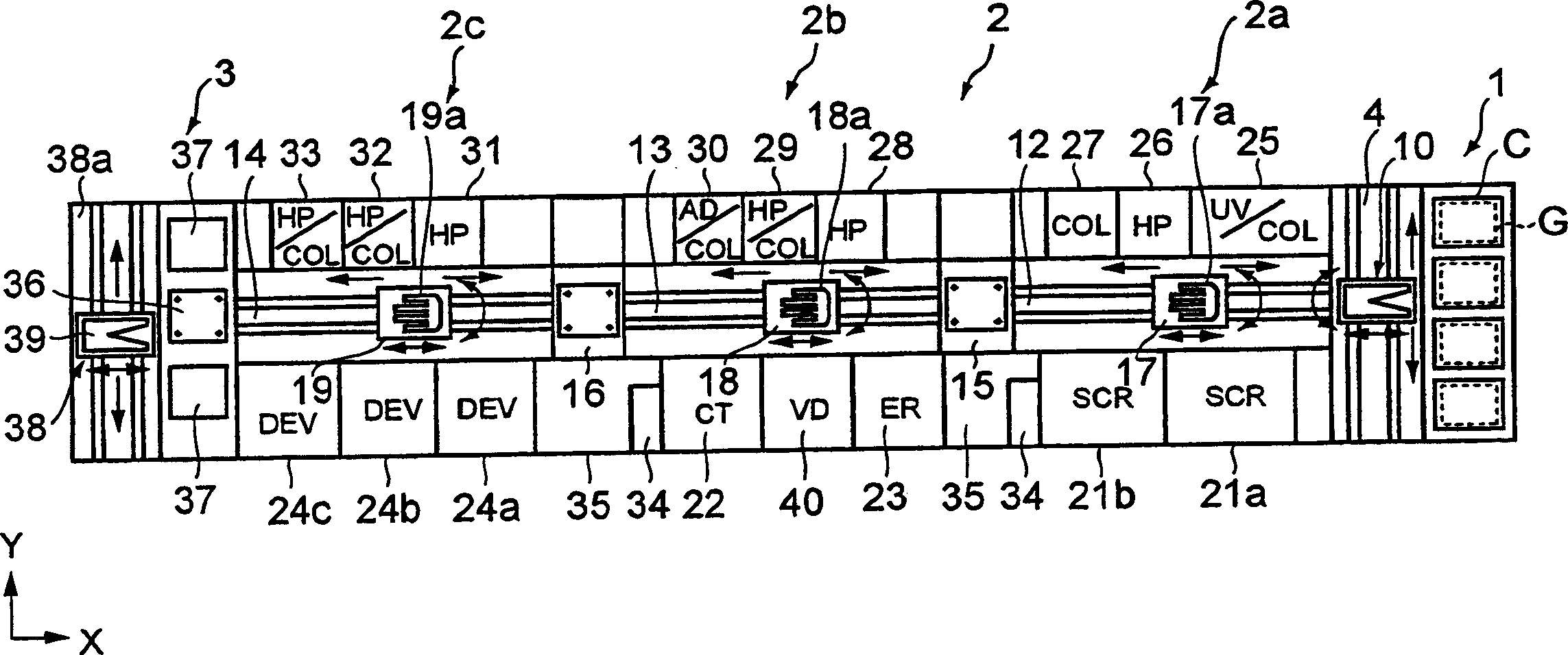
[0041] figure 1 It is a plan view showing the coating development processing system related to the first embodiment of the present invention. This coating and development processing system includes: a cassette table 1 on which a plurality of cassettes C for accommodating glass substrates G are placed; The processing section 2 of the unit; the interface section 3 for transferring the substrate G between the exposure device (not shown in the figure), and the cassette table 1 and the interface section 3 are respectively arranged at both ends of the processing section 2.
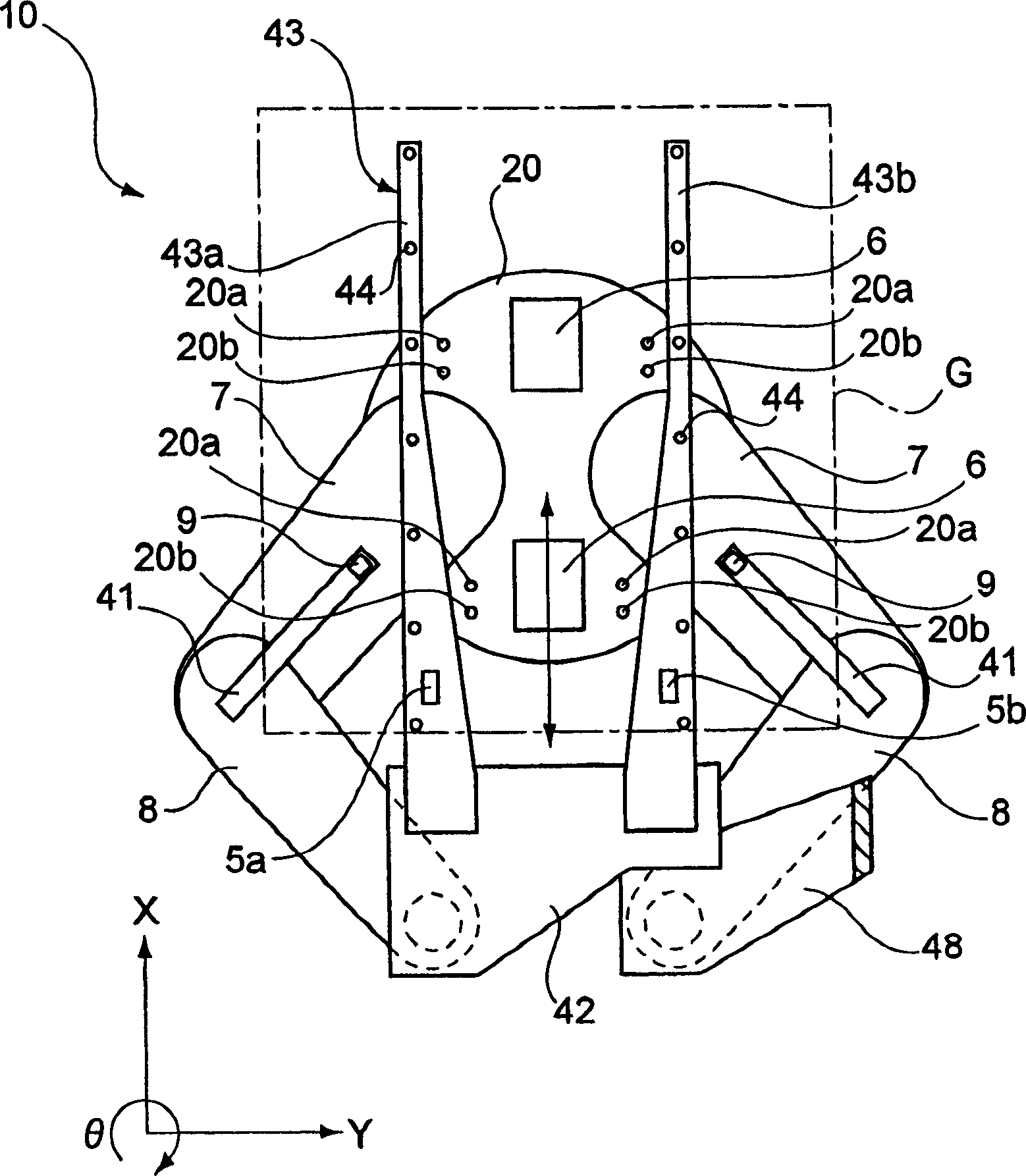
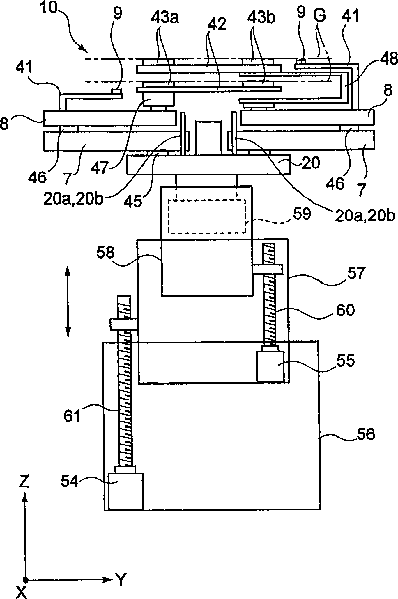
[0042] The cassette station 1 includes a transport device 10 having a articulated support arm related to the first embodiment of the present invention. The transport device 10 moves along the transport line 4 and transports the substrate G between the cassette C and the processing unit 2 . The transfer device 1...
PUM
 Abstract
Description
Claims
Application Information