Method for forming porous dielectric material layer on semiconductor device and formed device

A technology of dielectric material layer and dielectric material, which is applied in semiconductor/solid-state device components, semiconductor devices, semiconductor/solid-state device manufacturing, etc.

Inactive Publication Date:
View PDF0 Cites 9 Cited by
  • Summary
  • Abstract
  • Description
  • Claims
  • Application Information

AI Technical Summary

Problems solved by technology

However, problems arise when using porous dielectric materials, i.e. when these materials are first formed in electronic devices and then undergo a patterning process by means of reactive ion etching (RIE).

Method used


Image

  • Method for forming porous dielectric material layer on semiconductor device and formed device
  • Method for forming porous dielectric material layer on semiconductor device and formed device
  • Method for forming porous dielectric material layer on semiconductor device and formed device

Examples


Embodiment Construction

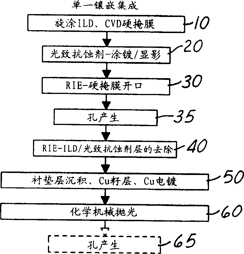
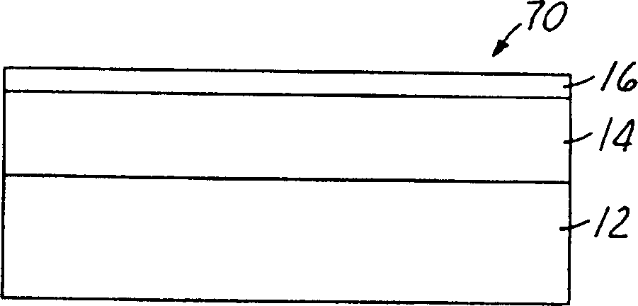
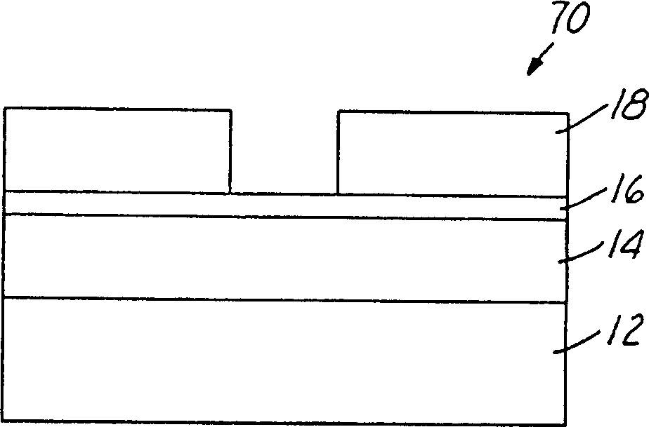
[0029]The invention discloses a method for forming a dielectric material layer in an electronic structure, more particularly, discloses a method for forming a porous dielectric material layer in an electronic structure, the method first forms a non-porous dielectric material layer , followed by local curing, patterning, and finally curing the layer at a temperature higher than the local curing temperature to transform the non-porous dielectric material into a porous dielectric material.

[0030] The method is carried out by the following steps: first providing a pre-processed semiconductor wafer, depositing a non-porous dielectric material layer on the pre-processed semiconductor wafer, curing the semiconductor wafer at a first temperature not higher than 350°C, defining and The layer of nonporous dielectric material is patterned and the semiconductor wafer is cured at a second temperature higher than the first temperature to convert the nonporous dielectric material into a por...


PUM

PropertyMeasurementUnit
thicknessaaaaaaaaaa
thicknessaaaaaaaaaa

Abstract

A method for forming a porous dielectric material layer in an electronic structure and the structure formed are disclosed. In the method, a porous dielectric layer in a semiconductor device can be formed by first forming a non-porous dielectric layer, then partially curing, patterning by reactive ion etching, and final curing the non-porous dielectric layer at a higher temperature than the partial curing temperature to transform the non-porous dielectric material into a porous dielectric material, thus achieving a dielectric material that has significantly improved dielectric constant, i.e. smaller than 2.6. The non-porous dielectric material may be formed by embedding a thermally stable dielectric material such as methyl silsesquioxane, hydrogen silsesquioxane, benzocyclobutene or aromatic thermoset polymers with a second phase polymeric material therein such that, at the higher curing temperature, the second phase polymeric material substantially volatilizes to leave voids behind forming a void-filled dielectric material.

Description

technical field [0001] The present invention relates generally to methods of forming layers of dielectric material on electronic structures and the structures formed, and more particularly to methods of forming layers of porous dielectric materials on electronic structures and electronic structures formed from such materials, the method A layer of non-porous dielectric material is first formed, then locally cured, patterned, and finally cured at a higher temperature than used in the partial cure to convert the non-porous dielectric material to a porous dielectric material. Background technique [0002] In the recent development of semiconductor devices, the continuous miniaturization of devices requires the use of electronic materials with superior properties. For example, dielectric materials used as insulating layers in semiconductor devices must have lower dielectric constants to provide less signal propagation delay. Thus, it is important to prov...

Claims


Application Information

Patent Timeline
Patent Type & Authority Applications(China)
IPC IPC(8): H01L21/31H01L21/316H01L21/768H01L23/532
CPCH01L21/76802H01L21/76828H01L21/31695H01L21/02362H01L21/02126H01L21/7682H01L21/02203H01L23/5329H01L2924/0002H01L2221/1047H01L2924/00H01L21/31
Inventor 蒂莫西·J·多尔顿斯蒂芬·E·格雷科杰弗里·C·赫德里克萨泰亚纳雷亚纳·V·尼塔桑佩思·珀鲁肖瑟曼肯尼思·P·罗德贝尔罗伯特·罗森堡
Why Eureka
Try Eureka