

Thermal-oxidative production process of semiconductor wafer
A manufacturing process and thermal oxidation technology, applied in semiconductor/solid-state device manufacturing, electrical components, circuits, etc., to achieve the effect of improving the pass rate
- Summary
- Abstract
- Description
- Claims
- Application Information
AI Technical Summary
Problems solved by technology
Method used
Image

Examples
Embodiment Construction
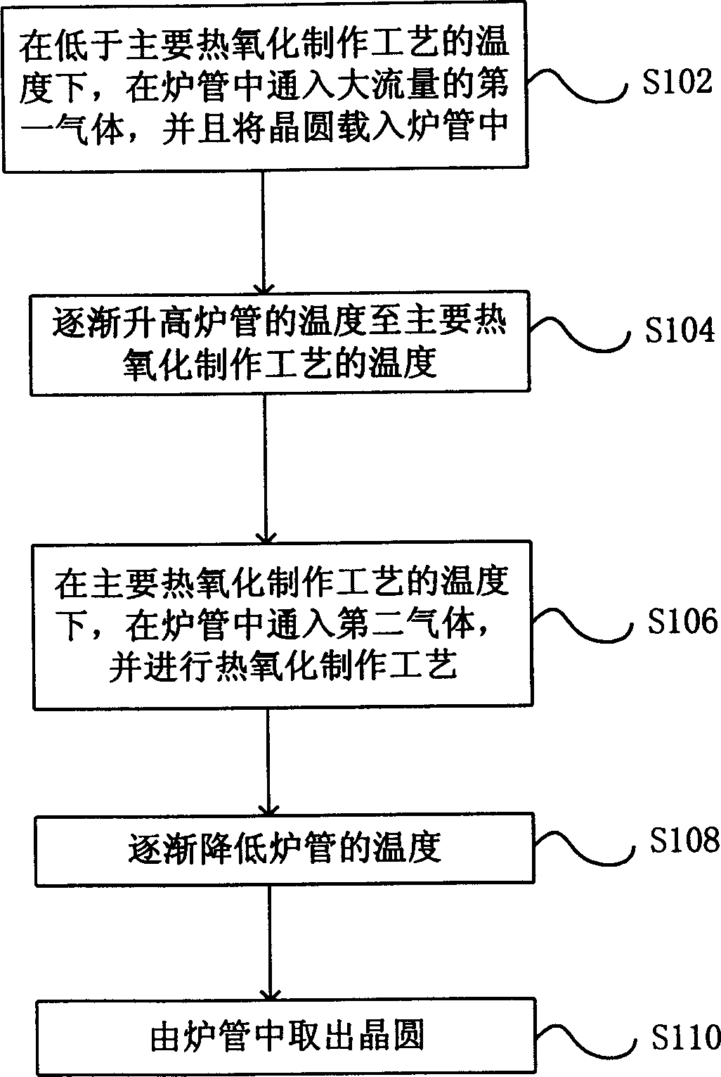
[0023] figure 1 Shown is a schematic flow chart of a thermal oxidation manufacturing process of a semiconductor wafer according to a preferred embodiment of the present invention, and the steps for forming an oxide layer are as follows:
[0024] Step 102: Load the wafers into the furnace tube, where several wafers can be placed in a boat, and then load the wafer into the furnace tube. In the step of loading the wafer into the furnace tube, the temperature during the loading of the wafer is lower than the temperature of the main thermal oxidation process, such as about 400 to 600 degrees Celsius, and while the wafer is being loaded, the A first gas with a large flow rate sufficient to drive away moisture and oxygen in the furnace tube is passed into the furnace tube, wherein the first gas is, for example, nitrogen or argon, and its flow rate is about 30 to 45 liters per minute, and the passed The concentration of the first gas entering is greater than 99.99%.
[0025] Since i...
PUM
 Abstract
Description
Claims
Application Information