Semiconductor devices
A semiconductor and device technology, applied in the field of semiconductor devices, can solve problems such as high temperature melting, flow away, and reducing the reliability of semiconductor devices
- Summary
- Abstract
- Description
- Claims
- Application Information
AI Technical Summary
Problems solved by technology
Method used
Image

Examples
Embodiment Construction
[0029] Embodiments according to the present invention will be described in detail below with reference to the accompanying drawings.
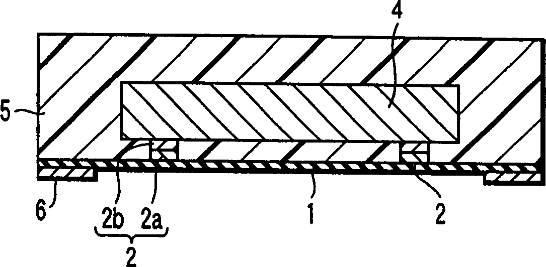
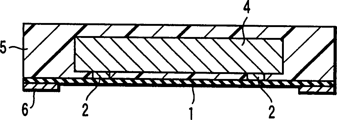
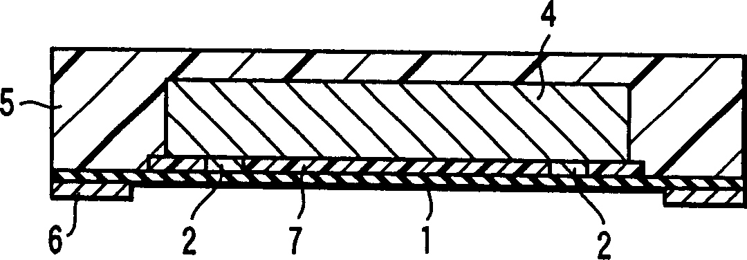
[0030] figure 2 A cross-sectional view of a semiconductor device according to one embodiment of the present invention is shown.
[0031] In the semiconductor component shown here, a semiconductor chip 4 is mounted on the surface of a substrate 1 via an electrically conductive connection part 2 . The substrate 1 may be formed of polyimide tape or ceramics, and has terminals 6 for external connection on its lower surface.
[0032] Although not shown in the drawings, the conductive connection member 2 is composed of bumps for the semiconductor chip 4 and bumps for the wiring circuit terminals of the substrate 1 . These bumps may be formed of, for example, tin / silver solder, gold, tin / lead solder, tin, tin / silver / copper solder, tin / zinc solder, tin / bismuth solder, or nickel. The terminal 6 for external connection can be formed of, for example, ...
PUM
| Property | Measurement | Unit |
|---|---|---|
| thickness | aaaaa | aaaaa |
| thickness | aaaaa | aaaaa |
| diameter | aaaaa | aaaaa |
Abstract
Description
Claims
Application Information