Semiconductor device and microprocessor

A microprocessor and semiconductor technology, applied in the direction of semiconductor devices, semiconductor/solid-state device components, electric solid-state devices, etc., can solve the problems that it is difficult to draw fine patterns on large-size glass substrates at high speed, and it is impossible to suppress the size of TFTs. Achieve the effect of suppressing cost increase, suppressing quantity increase, and easy structure

Inactive Publication Date: 2003-11-26
SEMICON ENERGY LAB CO LTD
View PDF0 Cites 3 Cited by
  • Summary
  • Abstract
  • Description
  • Claims
  • Application Information

AI Technical Summary

Problems solved by technology

Therefore, in the case of attempting to manufacture an integrated circuit using polycrystalline TFTs, it is impossible to suppress the size of the TFTs when attempting to obtain a sufficient on-state current
In addition, it is difficult to draw fine patterns at high speed on large-sized glass substrates, and these problems have become a bottleneck for achieving greater integration of integrated circuits

Method used


Image

  • Semiconductor device and microprocessor
  • Semiconductor device and microprocessor
  • Semiconductor device and microprocessor

Examples


example 1

[0052] In this example, an example will be described below in which a CPU core of a CPU (Central Processing Unit) typified by a microprocessor is formed on a plurality of glass substrates and the respective substrates are connected to optical interconnections.

[0053] TFTs formed on glass substrates operate slower than single crystal transistors. Therefore, in the case where the CPU is formed on a glass substrate, when the processing content becomes complicated, it is difficult for a single CPU core to perform processing at a sufficient speed. Then, a series of processing steps of the CPU core is divided into several processing steps according to each purpose, and the CPU core formed on one substrate is allocated to each processing step. Thus, a series of processing steps can be performed, similar to the case of using a single CPU core by connecting a plurality of substrates on which each CPU core is formed by optical interconnection. A CPU core formed on each substrate can ...

example 2

[0067] In this example, an example of a semiconductor display device which is one of the semiconductor devices of the present invention will be described below.

[0068] exist Figure 5 In , the structure of the semiconductor display device of this example is represented as a block diagram. Figure 5 In this method, two glass substrates are used. On the first substrate 200, an external input terminal 225, a VRAM (Video Random Access Memory) 201, a time signal generation circuit 202, an image signal processing circuit 203, and a control signal processing circuit 203 are provided. The light output section 204 for the image signal and the light output section 205 for the image signal.

[0069] One or more light emitting elements 220 and a light emitting element driving section 221 corresponding to the one or more light emitting elements 220 are formed at the light output section 204 for control signals and the light output section 205 for image signals, respectively. It should ...

example 3

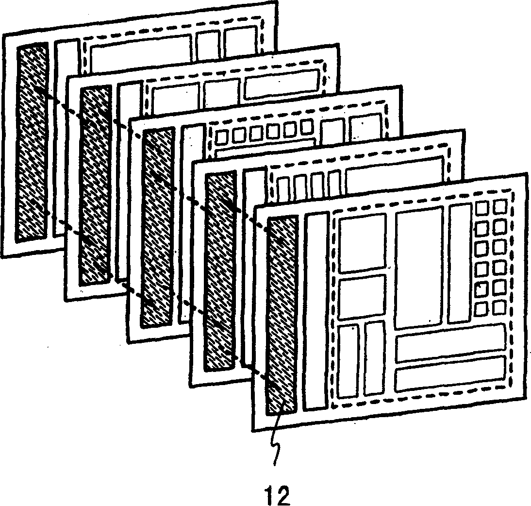
[0100] In this example, an example of how substrates on which circuits are formed are stacked layer by layer will be described below.

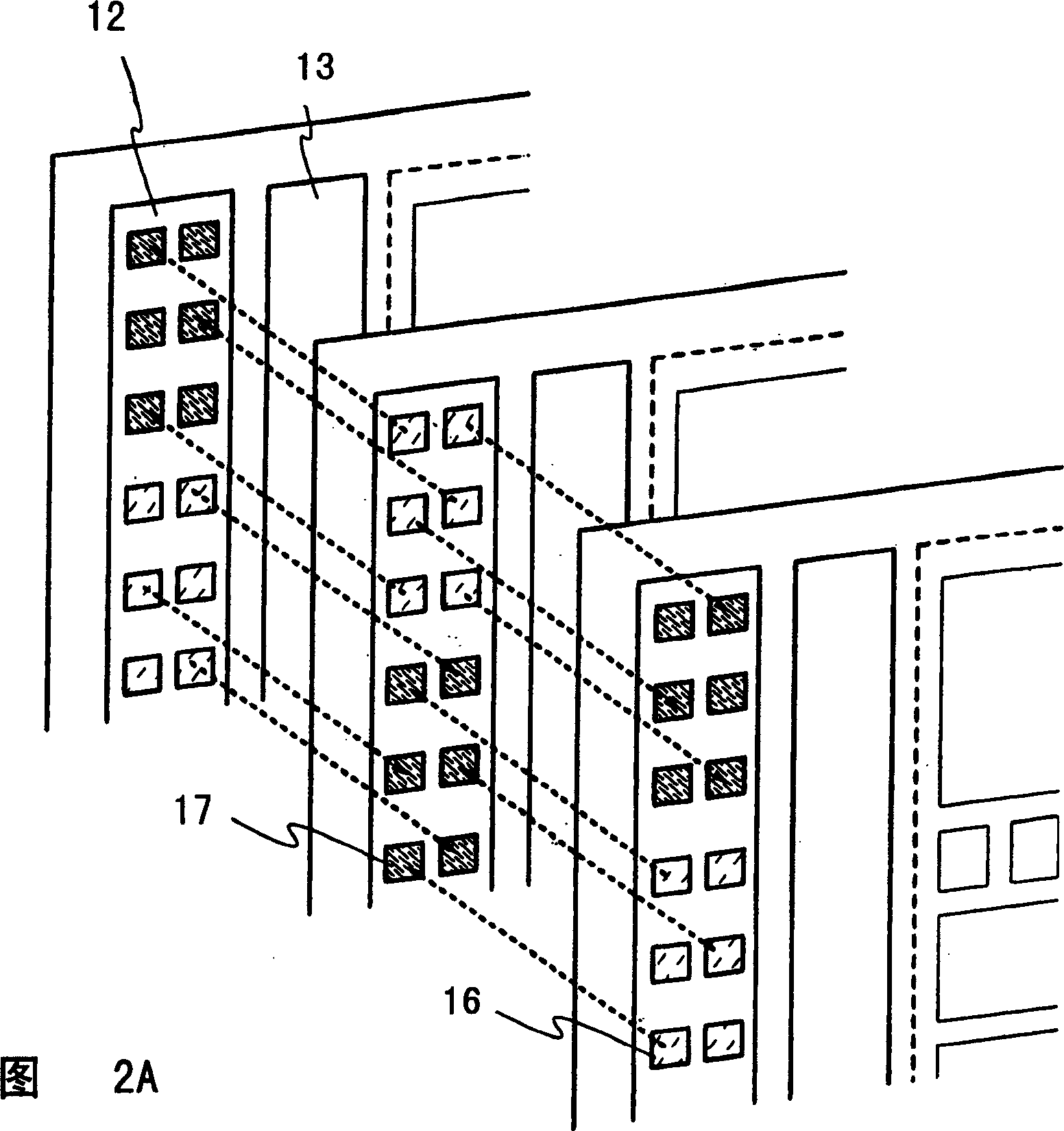
[0101] exist Figure 8A In , an example of a cross-sectional view of the semiconductor device of this example is shown. The light input part 301 and the light output part 302 are provided on a plurality of substrates 300 . In addition, an adhesive 304 is filled between the respective substrates, and a spacer 303 is used to fix the distance between the substrates.

[0102] It should be noted that the adhesive is not necessarily required to be filled between the substrates, and it is possible to partially use the adhesive so that air, inert gas, and other gases exist between the light input portion and the light output portion.

[0103] The light output portion 302 provided on each substrate corresponds to at least one light input portion 301 formed on another substrate 300 . Thus, in this example, the position of each substrate 300 in the ho...


PUM


Abstract

An object of the present invention is to provide a semiconductor device using a cheap glass substrate, capable of corresponding to the increase of the amount of information and further, having a high performance and an integrated circuit capable of operating at a high rate. A variety of circuits configuring an integrated circuit are formed on a plurality of glass substrates, the transmission of a signal between the respective glass substrates is performed by what is called an optical interconnect using an optical signal. Concretely, alight emitting element is provided on the output side of a circuit disposed on the upper stage formed on one glass substrate, and a photo-detecting element is formed so as to oppose to the relevant light emitting element on the input side of a circuit disposed on the rear stage formed on another glass substrate. Then, an optical signal converted from an electrical signal outputted from a circuit disposed on the upper stage is outputted from the light emitting element, the relevant optical signal is converted into an electrical signal by a photo-detecting element and inputted into a circuit disposed on the rear stage.

Description

technical field [0001] The present invention relates to a semiconductor device composed of a semiconductor film having a crystal structure formed on a glass substrate, and more particularly, the present invention relates to a semiconductor device for signal transmission in related devices through optical interconnection. Background technique [0002] Regarding the thin film transistor (TFT) formed on an insulating substrate or insulating film, it is characterized in that its manufacturing method is easy compared with the manufacturing method of a MOS (Metal Oxide Semiconductor) transistor formed on a silicon wafer, and it can utilize large Dimensional substrates make it at low cost. [0003] In particular, regarding a TFT (Thin Film Transistor) whose active layer is formed with a polycrystalline silicon film (in this case, a polycrystalline TFT), since its mobility is larger than that of a TFT using amorphous silicon, it is expected to be applied In a wide range of fields i...

Claims


Application Information

Patent Timeline
Patent Type & Authority Applications(China)
IPC IPC(8): H01L31/12G02B6/43H01L27/15
CPCH01L2225/06575H01L27/1214H01L2924/0002G09G3/3275G09G2360/14G02B6/43H01L25/0657H01L2225/06551G09G2370/08H01L2225/06527H01L27/124H01L27/1248H01L2924/00G02B6/12
Inventor 山崎舜平加藤清荒井康行秋叶麻衣
Owner SEMICON ENERGY LAB CO LTD
Why Eureka
Try Eureka