

An organic light-emitting device structure using metal cathode sputtering
A device and anode technology, applied in the field of organic light-emitting device structure using metal cathode sputtering, can solve the problems of manufacturing uniform and high-quality targets, and achieve the effect of large manufacturing tolerance and small damage
- Summary
- Abstract
- Description
- Claims
- Application Information
AI Technical Summary
Problems solved by technology
Method used
Image

Examples
Embodiment 1
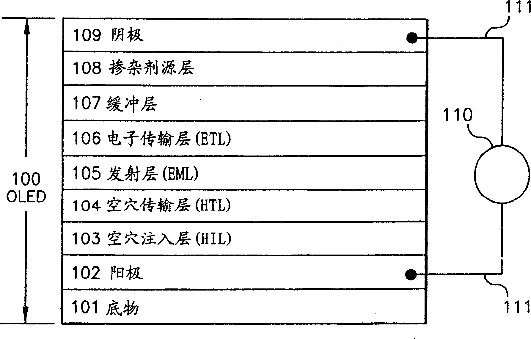
[0059] Table 2 collects the buffer layer and cathode structure of the organic EL medium, the performance of the device obtained in the present invention, and the related conditions of the control device. The ITO, HIL, HTL, and EML / ETL layers of devices 20 and 21 were identical, and each organic layer was deposited with a single pump down. Control device 20 had a standard cathode consisting of a 70 nm thick Al layer on a 0.5 nm LiF layer, exhibiting a luminance of 538 cd / cm 2 And working voltage 5.5 volts. Device 21 had a 20 nm thick CuPc buffer layer on which was vapor deposited a 0.5 nm thick LiF layer. Fabrication of the device was accomplished by depositing a 50 nm thick Al layer by sputtering. Device 21 exhibits a luminance of 554cd / m 2 And working voltage 5.8V. Device 21 has practically the same operating voltage and luminous efficiency as standard device 20 . Standard devices were assumed to be undamaged during the evaporation deposition of the Al layer. It is theref...
Embodiment 2
[0062] Table 3 summarizes the buffer layer and cathode structures of the two devices 30 and 31 . Device 31 is fabricated in accordance with the present invention. The ITO, HIL, HTL, and EML / ETL layers of devices 30 and 31 were identical, and the organic layers were deposited down with a single pump. However, in this experiment, a 35 nm thick Alq EML / ETL thin layer was used instead of the commonly used 60 nm thick Alq. Device 30 had no LiF (dopant source) layer, but had a 20 nm thick CuPc buffer layer on which was sputter-deposited a 50 nm thick Al layer. The performance of the device is very poor, showing a luminance of only 9cd / m 2 And working voltage 8.2V. Based on the performance of device 21 (Table 2), it can be concluded that the 20 nm thick CuPc layer has excellent protection against sputtering damage, but device 30 has extremely poor performance without the dopant source layer. When a 0.5 nm thick LiF dopant source layer is provided on the CuPc layer, as in device 3...
Embodiment 3
[0066] Table 4 compiles the buffer layer and cathode structure of the organic EL medium, the performance of the device obtained in the present invention, and the related conditions of the control device. The ITO, HIL, HTL, and EML / ETL layers of devices 40 and 41 were identical, and each organic layer was deposited down with a single pump. But in this example, the thickness of the ITO anode layer is 85 nanometers instead of the usual 42 nanometers.
[0067] Control device 40, having a standard cathode comprising a 70nm thick layer of evaporated aluminum on a 0.5nm LiF layer, exhibited a luminosity of 679 cd / m 2 And working voltage 5.8 volts. The device 41 had a 30 nm thick CuPc buffer layer on which a 0.2 nm thick LiF layer was vapor deposited. Fabrication of the device was accomplished by sputter-depositing a 50 nm layer of Al. Device 41 exhibits a luminance of 585cd / m 2 And working voltage 6.0V. The operating voltage of device 41 is virtually identical to that of control...
PUM
| Property | Measurement | Unit |
|---|---|---|
| Thickness | aaaaa | aaaaa |
| Thickness | aaaaa | aaaaa |
| Thickness | aaaaa | aaaaa |
Abstract
Description
Claims
Application Information