Method for manufacturing organic electroluminescent display device

An electroluminescent display and manufacturing method technology, applied in the direction of electroluminescent light sources, electric light sources, lighting devices, etc., can solve the problem of low directivity of evaporation beams, reduction of evaporation beam density, and adverse effects on the characteristics of organic EL elements And other issues

Inactive Publication Date: 2004-04-14
SANYO ELECTRIC CO LTD
View PDF1 Cites 58 Cited by
  • Summary
  • Abstract
  • Description
  • Claims
  • Application Information

AI Technical Summary

Problems solved by technology

[0014] However, when the directivity of the evaporation beam is low, such as Figure 12A As shown, because of the so-called shadowing effect, the components of the evaporation beam obliquely incident from the edge of the opening 102 of the shield 101 are generated, and the area wider than the opening 102 is evaporated.
In addition, the density of the vapor deposition beam gradually decreases from the center of the opening 102 to the edge.
As a result, such as Figure 12B As shown, the vapor-deposited organic EL material layer 200 has an uneven film thickness in which the central part is thick and the peripheral part is thin, which adversely affects the characteristics of the organic EL element 60.

Method used


Image

  • Method for manufacturing organic electroluminescent display device
  • Method for manufacturing organic electroluminescent display device
  • Method for manufacturing organic electroluminescent display device

Examples


no. 1 Embodiment approach

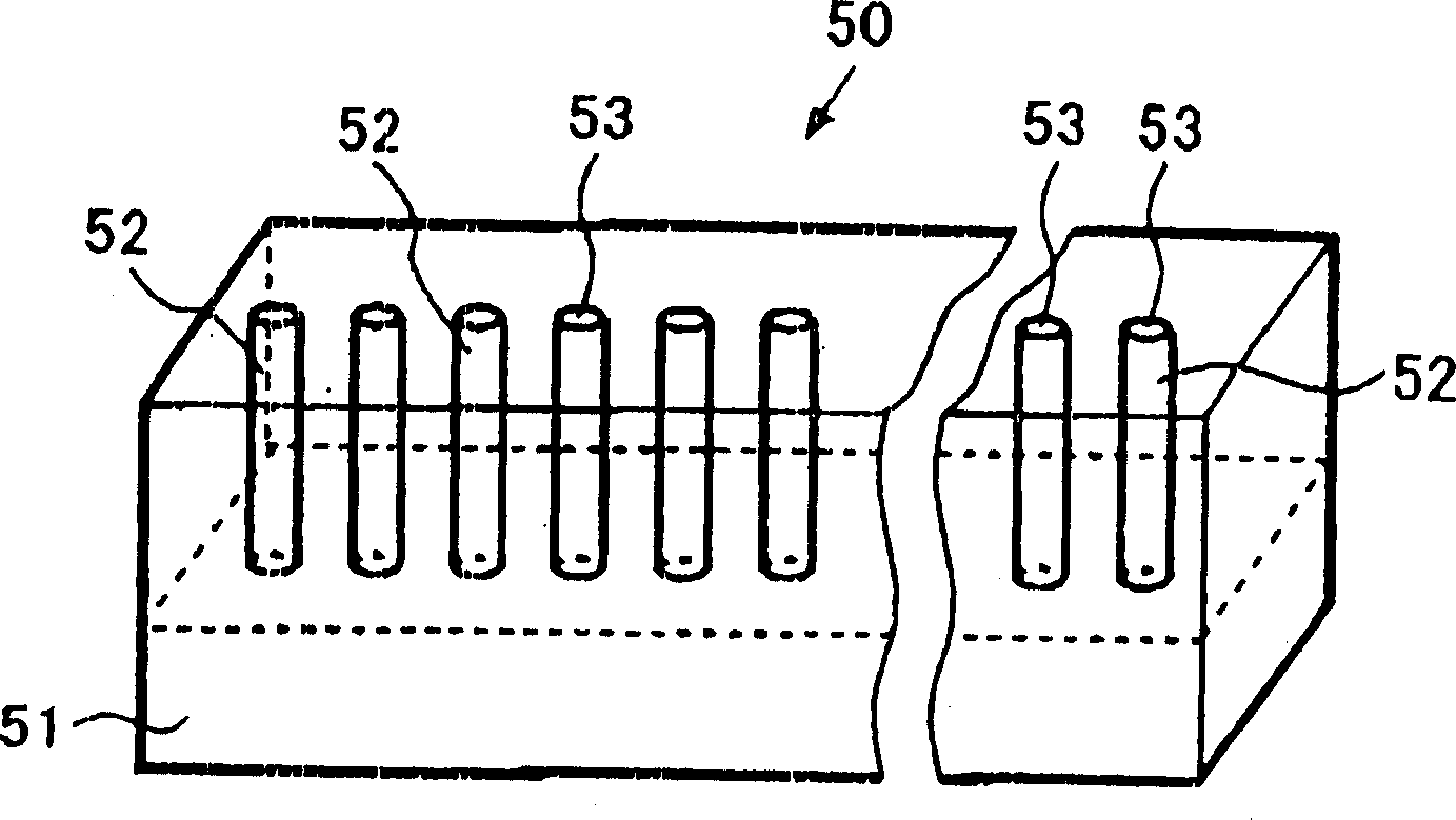
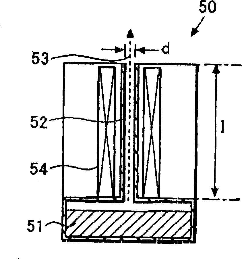
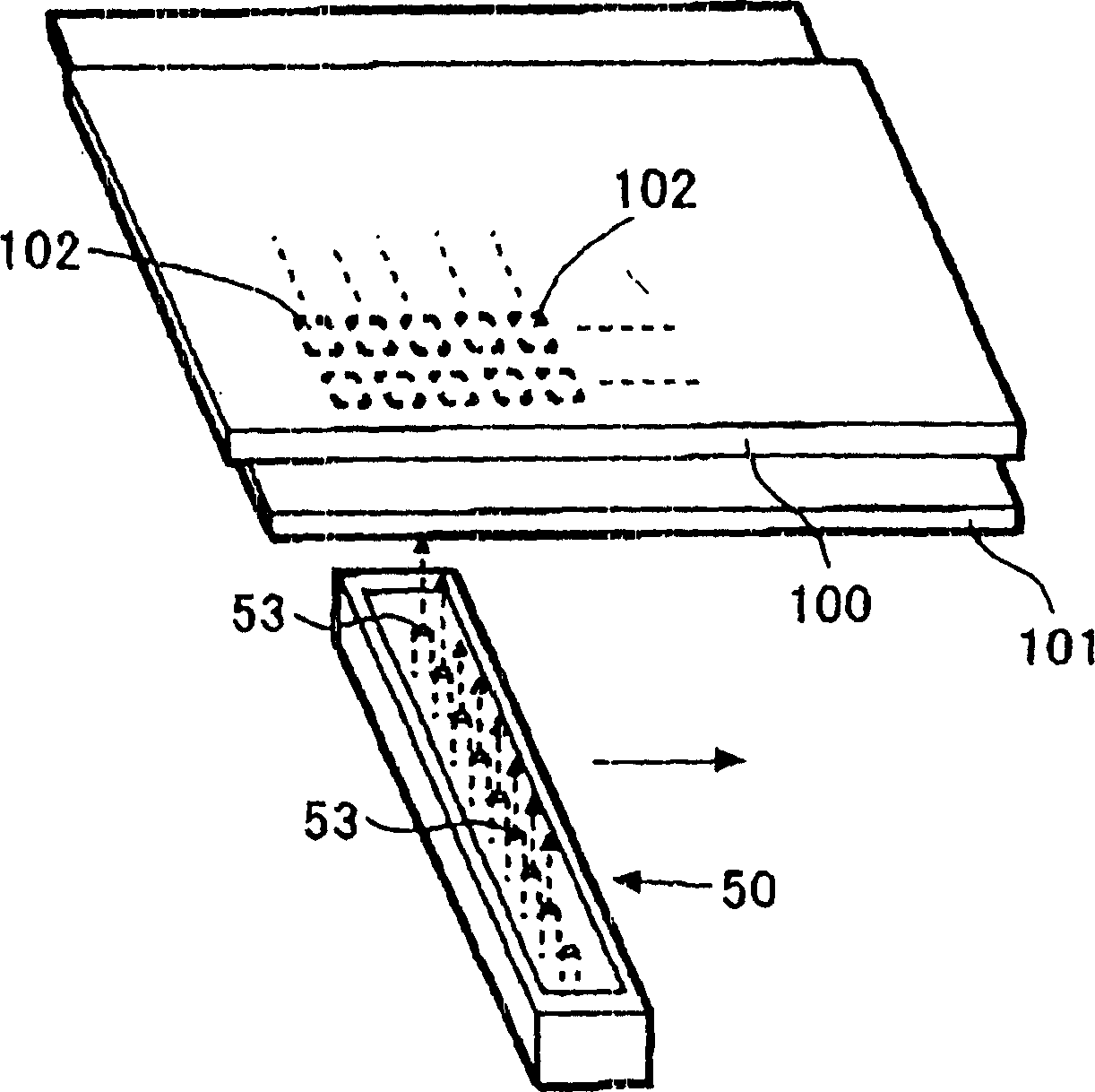
[0035] Hereinafter, the first embodiment of the present invention will be described in detail with reference to the accompanying drawings. figure 1 is a perspective view of the vapor deposition beam generating source 50, figure 2 for figure 1 sectional view, image 3 is a perspective view showing the vapor deposition process of the organic EL material, Figure 4 then image 3 sectional view.

[0036]In the method of manufacturing an organic EL display device of the present invention, an insulating substrate 10 is prepared in advance, and an organic EL element driving TFT and an organic EL element 60 are sequentially formed on the insulating substrate 10, except for the formation of the organic EL element 60. Except for the steps, the steps are the same as those described above.

[0037] The hole transport layer 62 , the light emitting layer 63 , the electron transport layer 64 , and the cathode 65 constituting the organic EL element 60 are patterned by vapor deposition...

no. 2 Embodiment approach

[0049] Hereinafter, a second embodiment of the present invention will be described in detail with reference to the accompanying drawings. Image 6 A perspective view of the vapor deposition beam generation source 150 and the vapor deposition beam direction adjustment plate 70 provided so as to face the vapor deposition beam generation source 150, Figure 7 for Image 6 sectional view, Figure 8 is a perspective view showing the vapor deposition process of the organic EL material, Figure 9 then Figure 8 sectional view.

[0050] In the method for manufacturing an organic electroluminescence display device of the present invention, an insulating substrate 10 is prepared in advance, and an organic EL element driving TFT and an organic EL element 60 are sequentially formed on the insulating substrate 10, except for the organic EL element 60. Except for the forming process of , it is the same as the process described above.

[0051] The hole transport layer 62 , the light emi...


PUM


Abstract

A vapor-depositing mask is disposed adjacent a surface of a substrate disposed in a vacuum chamber, vapor-depositing beams containing an organic EL material are generated by a vapor-depositing beam generator, the vapor-depositing beams pass through openings in the vapor-depositing mask, and the organic EL material is vapor-deposited in a predetermined region on the surface of the substrate. The vapor-depositing beams are guided through a plurality of vapor-depositing beam passing pipes provided in the vapor-depositing beam generator. Alternatively, the vapor-depositing beams generated by the vapor-depositing beam generator are guided through a vapor-depositing beam direction adjusting board having a plurality of vapor-depositing beam passing holes. This enhances directional uniformity of the vapor-depositing beams, thereby enabling making each film thickness of organic EL material layers uniform and thus enhancing precision of forming patterns of the layers.

Description

technical field [0001] The present invention relates to a method of manufacturing an organic electroluminescence display device, and in particular, to a method of manufacturing an organic electroluminescence display device including a vapor deposition step of an organic electroluminescence material. Background technique [0002] In recent years, organic electroluminescence display devices using organic electroluminescence (Electro Luminescence: hereinafter referred to as "organic EL") elements have been attracting attention as display devices that can replace CRTs and LCDs. Research and development of organic EL display devices including thin film transistors (Thin Film Transistor: hereinafter referred to as "TFT") that drive the switching elements of the organic EL elements are also progressing. [0003] Figure 11 It is a cross-sectional view showing one display pixel of an organic EL display device. This display pixel has a TFT for driving an organic EL element in the vi...

Claims


Application Information

Patent Timeline
Patent Type & Authority Applications(China)
IPC IPC(8): H05B33/10C23C14/04C23C14/12C23C14/24H01L51/40H01L51/50
CPCH01L51/5012C23C14/12H01L51/0011C23C14/243C23C14/042H10K71/166H10K50/11H05B33/10
Inventor 米田清
Owner SANYO ELECTRIC CO LTD
Why Eureka
Try Eureka