Method of forming isolation membrane in semiconductor device

A semiconductor and isolation film technology, which is used in semiconductor/solid-state device manufacturing, electrical components, circuits, etc., and can solve the problems of rounded top corners of difficult trenches and lack of polymer carbon sources.

Inactive Publication Date: 2004-05-26
SK HYNIX INC
View PDF0 Cites 3 Cited by
  • Summary
  • Abstract
  • Description
  • Claims
  • Application Information

AI Technical Summary

Problems solved by technology

However, if the pad nitride film is used as an etch mask after removing the photoresist pattern, there is a lack of carbon source for polymer generation
Therefore, it is more difficult to round the top corners of the trenches with polymer

Method used


Image

  • Method of forming isolation membrane in semiconductor device
  • Method of forming isolation membrane in semiconductor device
  • Method of forming isolation membrane in semiconductor device

Examples


Embodiment Construction

[0036] Reference will now be made in detail to the preferred embodiments of the present invention, examples of which are illustrated in the accompanying drawings, wherein like reference numerals designate like or like parts.

[0037] Figures 2A to 2E A cross-sectional view of a semiconductor device for explaining a method of forming an isolation film in a semiconductor device of a preferred embodiment of the present invention.

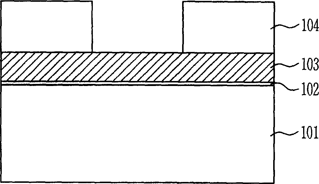
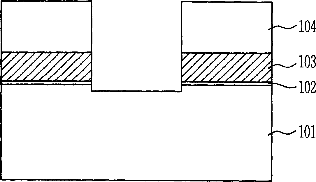
[0038] refer to Figure 2A A pad oxide film 202 and a pad nitride film 203 are sequentially formed on the semiconductor substrate 201 . Then photoresist covers the pad nitride film 203 . Next, exposure and development processes are performed to form a photoresist pattern 204, which defines an isolation region where an isolation film will be formed. Thereby, the pad nitride film 203 is exposed in the region where the isolation film is to be formed. At this time, the thickness of the pad nitride film 203 formed is preferably 1500 Å or less.

[0039] ...


PUM


Abstract

Disclosed is a method of forming an isolation film in a semiconductor device. In the process of forming a stack structure of a pad oxide film and a pad nitride film that expose a semiconductor substrate in an isolation region, protrusions of a tail profile are formed at the bottom sidewalls of the pad nitride film and the pad oxide film adjacent to the surface of the substrate, and top corners of a trench are made rounded using the protrusions as an anti-etch film when the substrate is etched, Therefore, it is possible to prevent concentration of an electric field on the top corners of the trench and prohibit generation of the leakage current. Accordingly, reliability of the process and electrical characteristics of the device could be improved.

Description

technical field [0001] The present invention relates to a method for forming an isolation film in a semiconductor device, more particularly, to a method for forming an isolation film capable of preventing electric field from concentrating on a shallow trench isolation (shallow trench isolation; STI) structure isolation film in a semiconductor device. method on the isolation membrane. Background technique [0002] In all semiconductor devices, an isolation film for electrically isolating various devices formed in a semiconductor substrate is formed. Traditionally, the isolation film is formed by means of a local oxidation (LOCOS) process. However, in this case, a beak shape appears at the top corner of the isolation membrane. As a result, there is a problem that the electrical characteristics and integration degree of the device are deteriorated. [0003] As semiconductor devices become more integrated, an isolation film should be formed to have an STI (Shallow Trench Isol...

Claims


Application Information

Patent Timeline
Patent Type & Authority Applications(China)
IPC IPC(8): H01L21/76H01L21/033H01L21/308H01L21/311H01L21/762
CPCH01L21/3086H01L21/0335H01L21/0337H01L21/3085H01L21/31116H01L21/76232H01L21/76
Inventor 李圣勋
Owner SK HYNIX INC
Why Eureka
Try Eureka