Magnetic memory and its drive method, and magnetic memory apparatus using same

A magnetic storage and driving method technology, applied in the field of magnetic storage devices, can solve the problems of impedance rise, magnetization reversal magnetic field recording current increase, recording errors, etc., to suppress refinement, realize magnetization reversal, and smooth magnetization reversal Effect

Inactive Publication Date: 2004-09-15
PANASONIC CORP
View PDF0 Cites 5 Cited by
  • Summary
  • Abstract
  • Description
  • Claims
  • Application Information

AI Technical Summary

Problems solved by technology

[0004] 1. Recording errors due to magnetic crosstalk due to reduced element spacing
[0005] 2. Increase in magnetization reversal magnetic field and increase in recording current due to finer magnetic materials
[0006] 3. Limitation of recording current due to miniaturization of wires
[0007] 4. With the miniaturization of wires, the impedance increases and the S / N decreases during readout
[0008] Because of these problems, it is generally believed that it is difficult to achieve high integration levels greater than Gbit / square inch

Method used


Image

  • Magnetic memory and its drive method, and magnetic memory apparatus using same
  • Magnetic memory and its drive method, and magnetic memory apparatus using same
  • Magnetic memory and its drive method, and magnetic memory apparatus using same

Examples


Embodiment 1

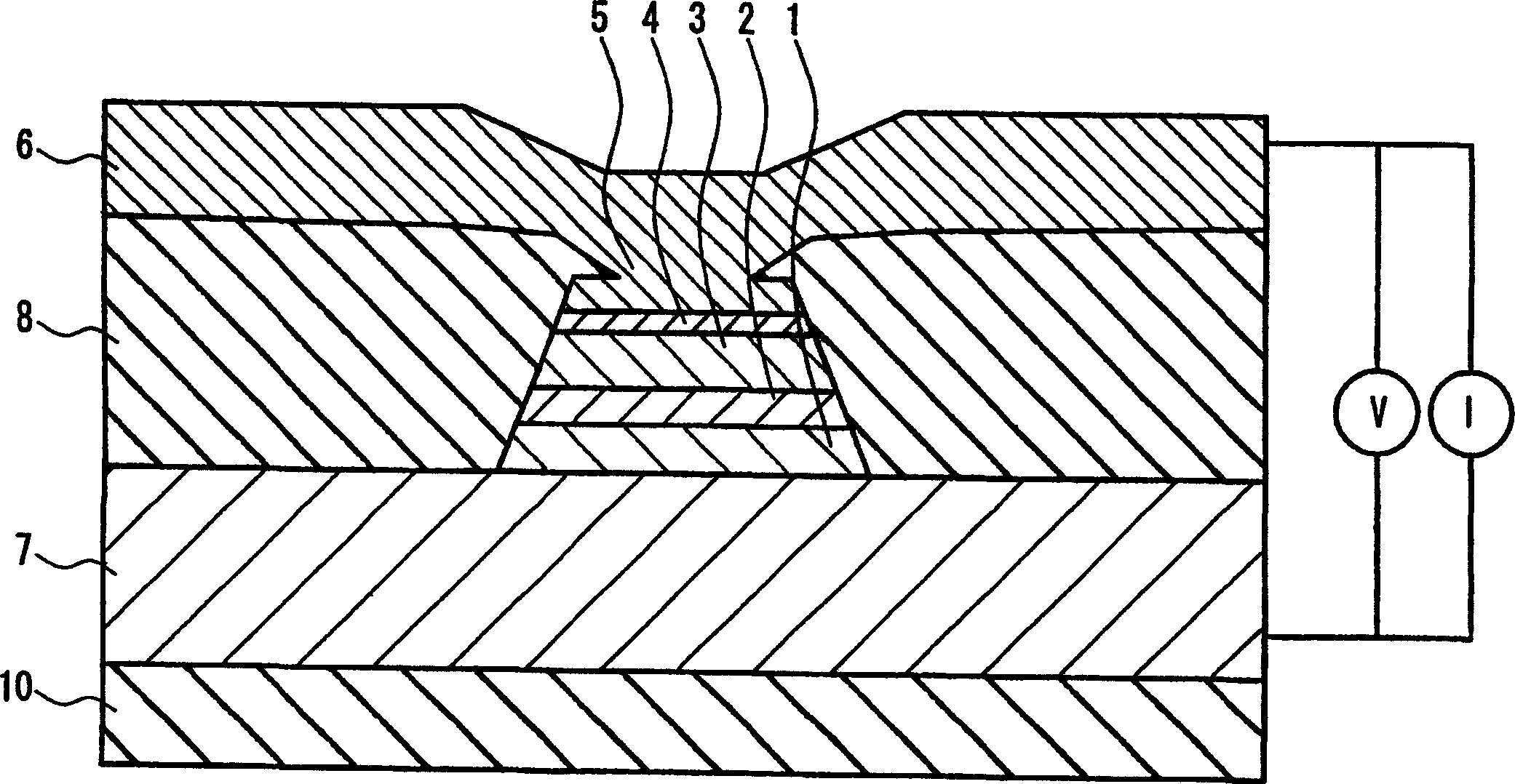
[0138] As shown in FIG. 3 , on a CMOS substrate, an integrated memory is fabricated using a magnetic memory composed of three stages of magnetoresistive elements. The integrated memory is sealed into a ceramic package, and a NiFe film with a thickness of 100 μm is plated on the entire package as a magnetic shield.

[0139] and Figure 11 The same as shown, the magnetic memories are arranged in a matrix shape, and every other storage column is configured with magnetic memories R1, R2, R3...( Figure 24 ). These magnetic memories also consist of 3-segment magnetoresistive elements. The magnetic memory is arranged in a manner of 256×256 (the total number of magnetoresistive elements is 256×256×3). There are 256 magnetic memories for comparison.

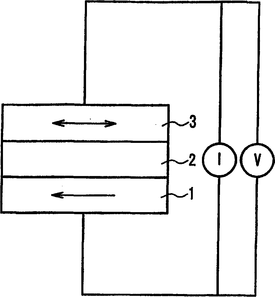
[0140] In each magnetic memory, a layered structure shown below was fabricated as a first-stage magnetic memory element.

[0141] Lower electrode / Ta(3) / PtMn(20) / CoFe(3) / Ru(0.9) / CoFe(3) / AlO(1.0) / NiFe(2) / AlO(1.0) / CoFe(3) / Ru( 0.9) / CoF...

Embodiment 2

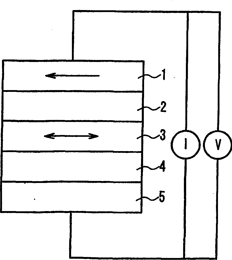
[0157] On a CMOS substrate, the pass will consist of a Figure 7 The magnetic memory composed of the magnetoresistive elements of the two memory layers 3 and 73 shown is arranged in a matrix to form an integrated memory. The same magnetic shielding as in Embodiment 1 is performed on the integrated memory. but, Figure 7 In the layers shown, the offset tunnel layers 4, 74 at both ends are omitted.

[0158] The arrangement of magnetic memory is identical with embodiment 1 ( Figure 24 ). In this integrated memory, the total number of memories is 256×256×2. This integrated memory is regarded as one frame, and a total of eight frames of MRAM are produced.

[0159] The film structure of the magnetoresistive element is as follows: lower electrode / Ta(3) / NiFeCr(4) / NiFe(2) / AlO(1.0) / CoFe(3) / Ru(0.8) / CoFe(3) / PtMn(20) / CoFe(3) / Ru(0.8) / CoFe(3) / AlO(1.06) / NiFe(2) / NiFeCr(4) / Ta(3) / upper electrode.

[0160] In this device, the tunnel layer and the memory layer are formed of AlO and NiFe, ...

Embodiment 3

[0169] On a glass substrate, an integrated memory was fabricated using a magnetic memory composed of three segments of magnetoresistive elements as shown in FIG. 9 . The same magnetic shielding as in Embodiment 1 is applied to the integrated memory.

[0170] Magnetic memory according to Figure 24 Arranged as shown. The magnetic memories are arranged in the form of 256×256 (the total number of magnetoresistive elements is 256×256×3), and these magnetic memory groups are regarded as one frame, and a total of 8 frames of MRAM are produced.

[0171] Among the three elements, the film structure of the magnetoresistive element is as follows:

[0172] Lower electrode / Ta(3) / PtMn(20) / CoFe(3) / Ru(0.9) / CoFe(3) / AlO(1.0) / Fe(2) / AlO(1.3) / Ta(3) / Upper electrode .

[0173] In this device, the tunnel layer and the memory layer are formed of AlO and Fe, respectively. AlO in contact with Ta is a bias tunneling layer.

[0174] This multilayer film is heat-treated in the same manner as in Exam...


PUM


Abstract

A magnetic memory of the present invention includes two or more memory layers and two or more tunnel layers that are stacked in the thickness direction of the layers. The two or more memory layers are connected electrically in series. A group of first layers includes at least one layer selected from the two or more memory layers. A group of second layers includes at least one layer selected from the two or more memory layers. A resistance change caused by magnetization reversal in the group of first layers differs from a resistance change caused by magnetization reversal in the group of second layers.

Description

technical field [0001] The present invention relates to a magnetic memory, a driving method thereof, and a magnetic storage device such as a magnetic random access memory (MRAM) using the memory. Background technique [0002] A tunnel magnetoresistance (TMR: tunnel magnetoresistance) element includes a tunnel (barrier layer: barrier) layer and a pair of magnetic layers sandwiching the layer. In the TMR element, the spin tunneling effect produced by the relative angle difference of the magnetization direction in a pair of magnetic layers is used. In the spin valve type TMR element, a pair of magnetic layers includes a fixed magnetic layer whose magnetization is hard to rotate and a free magnetic layer whose magnetization is easy to rotate. The free magnetic layer functions as a memory layer, and its information is recorded as a magnetization direction. [0003] As a magnetic memory, in an MRAM in which TMR elements are arranged in a matrix, as the integration level increase...

Claims


Application Information

Patent Timeline
Patent Type & Authority Applications(China)
IPC IPC(8): G11C11/00G11C11/15G11C11/16G11C11/22H01L21/8246H01L27/105H01L27/22
CPCG11C11/16B82Y10/00H01L27/224H01L27/228G11C11/5607G11C11/15G11C11/1659G11C11/161G11C11/1675G11C11/1693H10B61/10H10B61/22
Inventor 平本雅祥松川望小田川明弘里见三男杉田康成川岛良男
Owner PANASONIC CORP
Why Eureka
Try Eureka