Image display device and image display panel

An image display device and pixel technology, applied in static indicators, cathode ray tube indicators, optics, etc., can solve problems such as reference fluctuations, short sampling pulse periods, and decreased accuracy of feedback control

Inactive Publication Date: 2004-10-27
SONY CORP
View PDF0 Cites 2 Cited by
  • Summary
  • Abstract
  • Description
  • Claims
  • Application Information

AI Technical Summary

Problems solved by technology

The feedback IC 110 basically estimates the amount of deviation of the phase by using the potential difference between the power supply voltage Vdd and the ground potential GND (or a constant value close to it) as a reference, but in this case, the reference fluctuates up and down.
Therefore, the accuracy of the feedback control decreases and the timing of the clock is adjusted to a wrong value
[0019] As the number of horizontal pixels of the image display panel increases and the period of the sampling pulse becomes shorter, the decrease in the accuracy of the feedback control becomes significant
[0020] In addition, when the off-leakage of the TFT increases due to characteristic degradation, a current flows from the power supply voltage Vdd to the ground potential via the CMOS transmission gate 101 in an off state, and therefore, in the image display device or image The power loss in the display panel increases

Method used


Image

  • Image display device and image display panel
  • Image display device and image display panel
  • Image display device and image display panel

Examples


Embodiment Construction

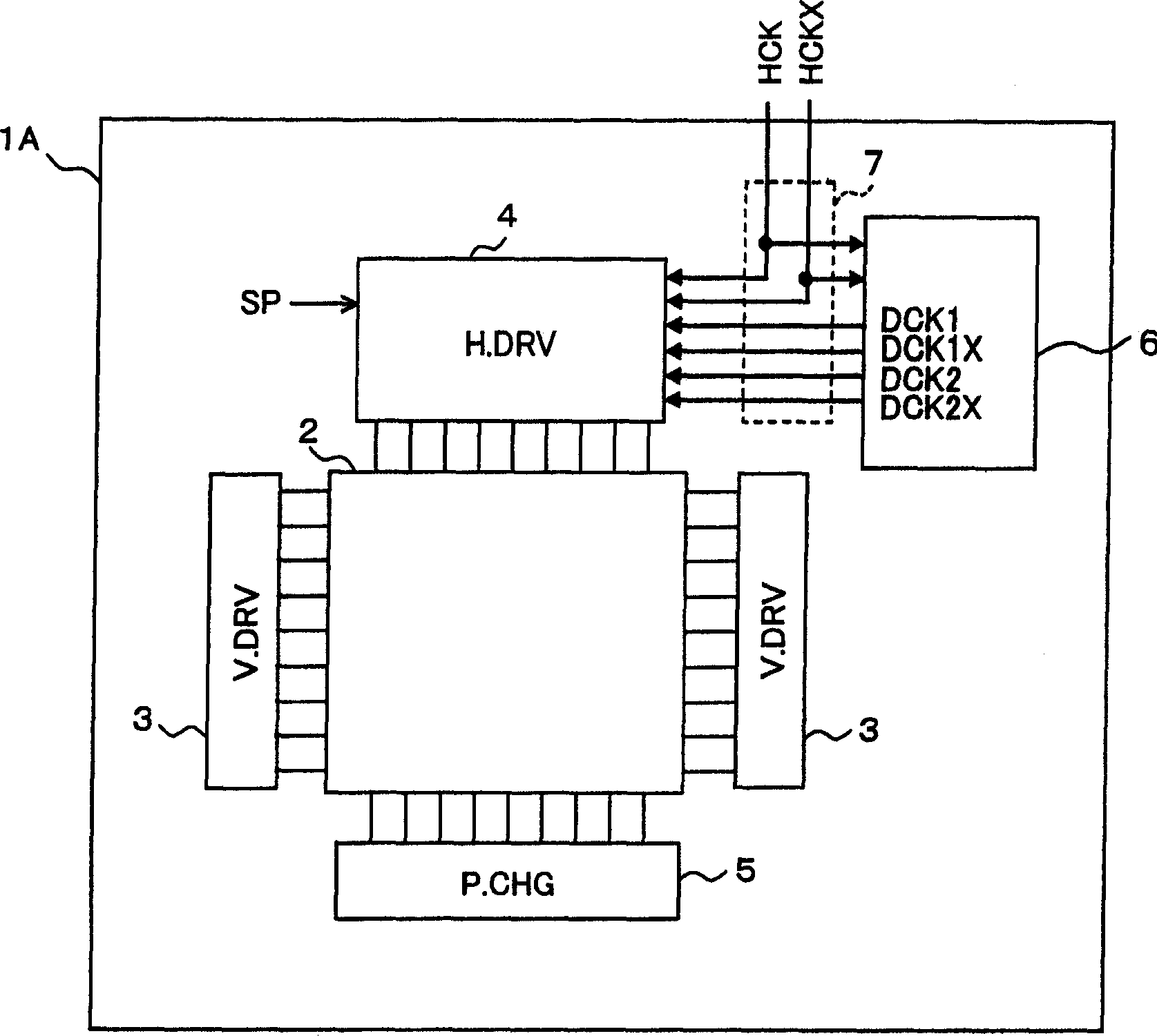
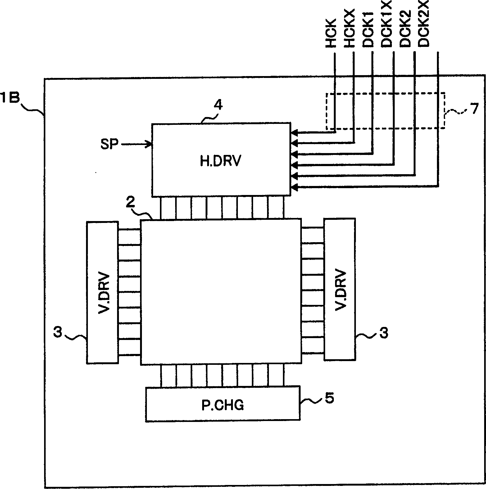
[0035] Hereinafter, embodiments in the present invention will be described by taking a liquid crystal display (LCD) as an example with reference to the accompanying drawings. The entire LCD panel has the same as figure 1 and figure 2 The same structure is shown in .

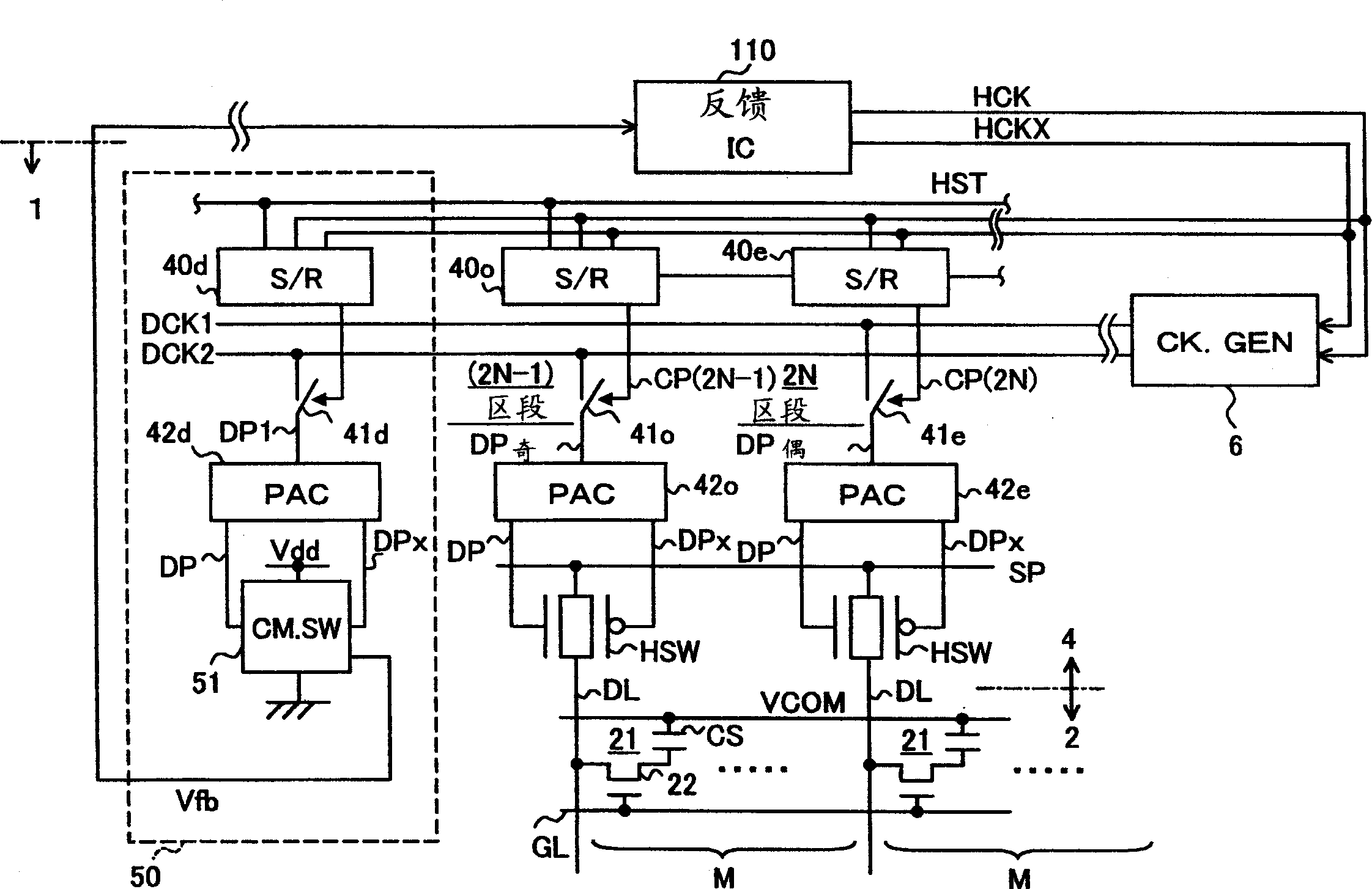
[0036] image 3 is a circuit diagram of a structural example of the liquid crystal panel 1 to which the dot timing clock driving system is applied. 4A to 4K are timing charts of waveforms of respective signals. notice, image 3 corresponds to figure 1 , and shows a clock generated internally.

[0037] For example, in the XGA specification, the pixel section 2 has a structure in which 1024*768 pixels 21 are arranged in a matrix. Each pixel 21 has a switching TFT 22, a holding capacitor Cs, and a liquid crystal cell (not shown). The holding capacitor Cs is formed between the pixel electrode connected to one of the source and drain of the TFT 22 and the power supply line of the common potential VCOM. The o...


PUM


Abstract

An image display device and an image display panel having high accuracy of adjusting sampling timing of a video signal and being capable of preventing a constant wasteful power consumption, comprise a timing detection circuit for generating a timing detection signal changing from a first level to a second level every time a switch circuit connected to each data line shared by pixels in each column sends a video signal, and the timing detection circuit includes at an output terminal of a timing detection signal a means (for example, PMOS) for closing a current path on the first level side and a means (for example NMOS) for opening a current path on the second level side respectively in synchronization with a video signal sending operation of the switch circuit.

Description

technical field [0001] The present invention relates to an image display device and an image display panel in which a so-called dot timing clock driving system is applied to a driving circuit. Background technique [0002] figure 1 and figure 2 is a block diagram of a structural example of an image display panel to which a dot timing clock driving system is applied. [0003] like figure 1 and figure 2 As shown, the image display panels 1A and 1B include a pixel portion 2 arranged in a matrix with pixels, a vertical drive circuit (V.DRV) 3, a horizontal drive circuit (H.DRV) 4, and a precharge circuit (P.CHG) 5 , as various circuits connected to the pixel portion 2. [0004] The pixel section 2 uses, for example, a liquid crystal element as a display unit (pixel) of an image. Each liquid crystal element has a liquid crystal cell and a thin film transistor (TFT) which is turned on at the time of display to supply a video signal SP to one electrode (pixel electrode) of ...

Claims


Application Information

Patent Timeline
Patent Type & Authority Applications(China)
IPC IPC(8): G02F1/133G03B21/00G03B33/12G09G3/20G09G3/36G09G5/18
CPCG09G3/3688G09G2330/021G09G2320/0209G09G3/20G09G2310/08G09G2310/0275G09G3/36
Inventor 原野环
Owner SONY CORP
Why Eureka
Try Eureka