LED

A technology of light-emitting diodes and diodes, applied in the direction of electrical components, circuits, semiconductor devices, etc., can solve the problems of not being in the same horizontal position, loss of luminous area, and lower production qualification rate

Inactive Publication Date: 2005-01-12
OPTO TECH
View PDF0 Cites 31 Cited by
  • Summary
  • Abstract
  • Description
  • Claims
  • Application Information

AI Technical Summary

Problems solved by technology

[0008] For the placement of the first electrode 27, part of the epitaxial layer 235 must be removed, which will lose part of the luminescent area and reduce the luminous brightness
[0009] For the placement of the first electrode 27, part of the epitaxial layer 235 must be removed, which will cause the first electrode 27 and the second electrode 25 to be not at the same horizontal position, and relatively increase the difficulty in subsequent manufacturing.
[0010] Since part

Method used


Image

  • LED
  • LED
  • LED

Examples


Embodiment Construction

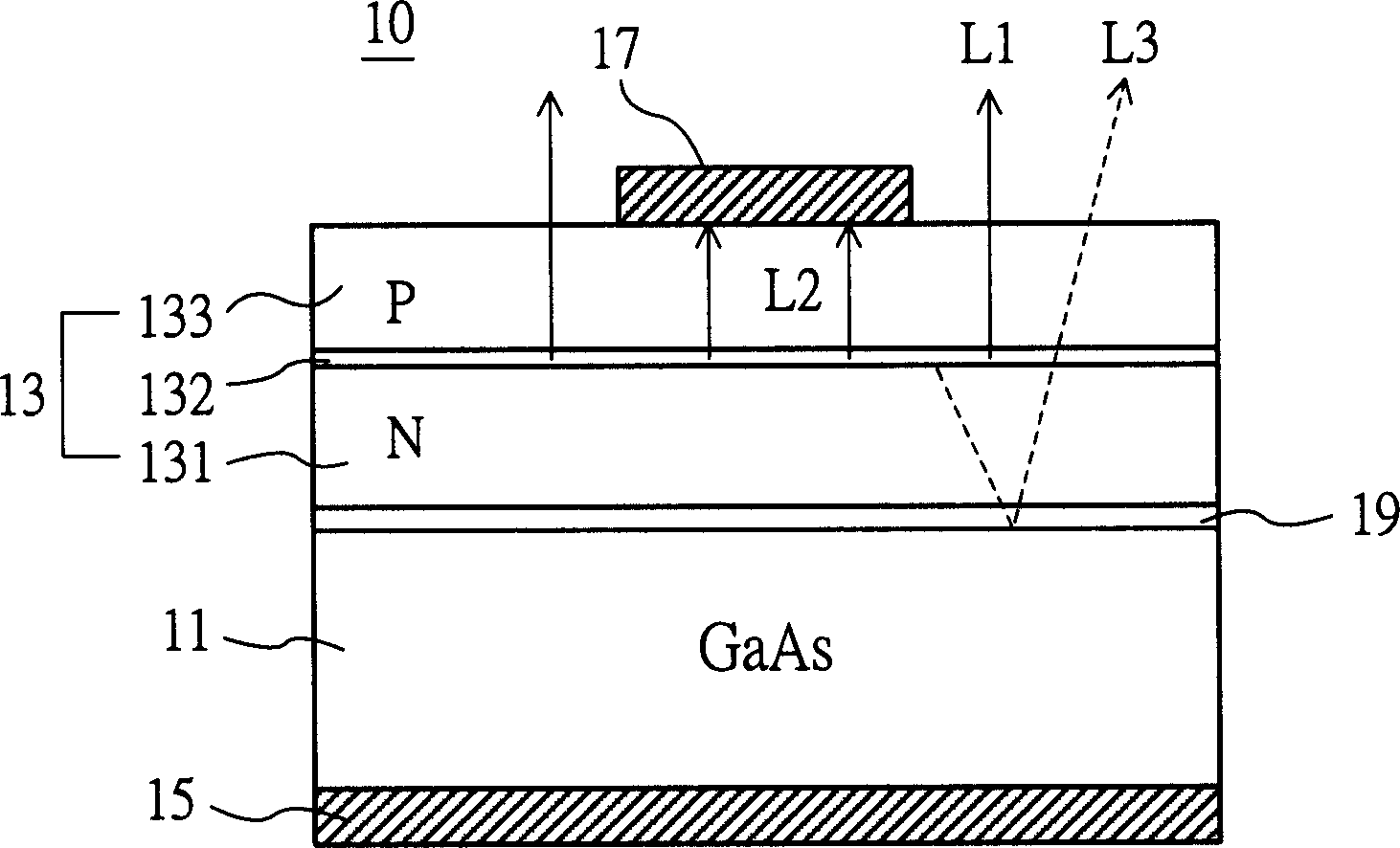
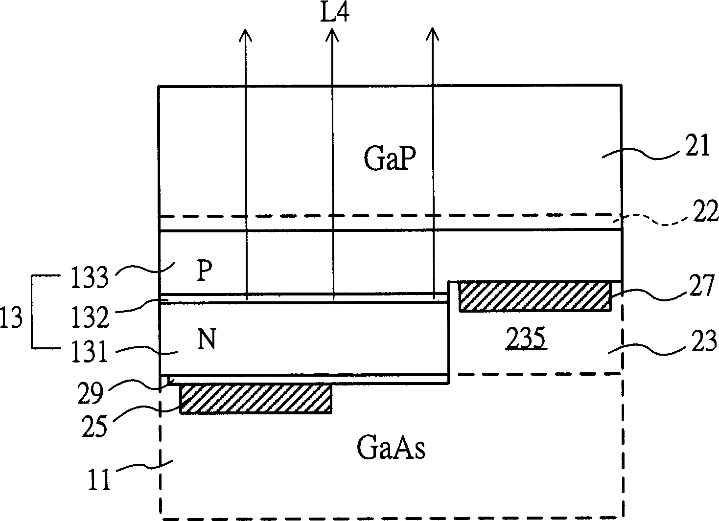
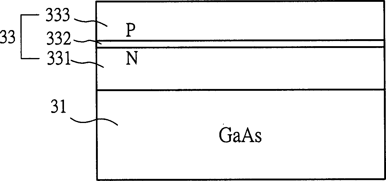
[0071] see Figure 3A to Figure 3C , are respectively the structural cross-sectional views of a preferred embodiment of the light-emitting diode of the present invention in each manufacturing step; as shown in the figure, the manufacturing of the present invention mainly includes the following steps:

[0072] First, a semiconductor substrate 31 is provided, such as a GaAs substrate (light-absorbing substrate), and a first material layer 331 (such as an N-type or P-type cladding layer), a light-emitting layer 332 and a second material layer are sequentially grown on the upper surface of the GaAs substrate 31. The material layer 333 (such as a P-type or N-type cladding layer), so as to form a quaternary epitaxial layer 33, as shown in FIG. 3A.

[0073] Wherein, the light-emitting layer 332 can be a PN interface, and can be optionally made of a ternary or quaternary compound, such as aluminum gallium arsenide (AlGaAs), aluminum gallium indium phosphide (AlGaInP) or aluminum galli...


PUM


Abstract

Quadreple epitaxial layer composed of first material layer, luminous layer and second material layer is formed on a semiconductor base plate. A euphotic base plate is fixed on surface of the second martial layer. With semiconductor base plate being removed, isolation groove and first extend groove are made under undersurface of first material to penetrate the first material layer and extend to part of volume of second material layer at least. First extend electrode is setup inside first extend groove. The first extend electrode is possible to connect with first electrode positioned at partial surface of the first material layer. Thus, the first electrode is located in nearly same level position to second electrode, which is on surface of other part of the first martial layer in order to carry out next processing easily. The invention increases luminescence are of PN interface, raises luminescence brightness and service life.

Description

technical field [0001] The invention relates to a light-emitting diode, especially a planar light-emitting diode that can be applied to a quaternary extension layer, which not only facilitates the subsequent manufacturing process, but also increases the luminous area of ​​the PN interface, thereby improving the luminous brightness and service life. Background technique [0002] Light-Emitting Diode (LED; Light-Emitting Diode) has been widely used in Indicator lights, advertising billboards, traffic lights, car lights, display panels, communication appliances, consumer electronics and other products. [0003] Existing light-emitting diodes, such as light-emitting diodes with quaternary epitaxial (epitaxy) layers, such as figure 1 As shown, the light-emitting component 10 mainly forms an epitaxial layer 13 on a semiconductor substrate 11 (such as a GaAs substrate), and the epitaxial layer 13 is formed by at least a first material layer 131, a light-emitting layer 132 and a s...

Claims


Application Information

Patent Timeline
IPC IPC(8): H01L33/00
Inventor 林明德许荣贵林三宝
Owner OPTO TECH
Why Eureka
Try Eureka