Capacitor arrangement

A capacitor structure, capacitor technology, applied in instruments, circuits, electrical components, etc., can solve the problems of insufficient pixel aperture ratio, decreased contrast, uncompetitiveness, etc., and achieve overall improvement in contrast deficiency, increased aperture ratio, and competitiveness. Effect

Inactive Publication Date: 2005-01-19
AU OPTRONICS CORP
View PDF0 Cites 5 Cited by
  • Summary
  • Abstract
  • Description
  • Claims
  • Application Information

AI Technical Summary

Problems solved by technology

Although a capacitor with a large-area electrode can store more charges to increase the time for the pixel to turn on, it will occupy a larger area, thereby reducing the aperture ratio of the pixel.
As a result, not only the maximum brightness that the LCD panel can achieve is limited, but the overall contrast is also reduced. At the same time, due to the limitation of insufficient pixel aperture ratio, special processing or consideration is often required when designing or producing products, resulting in Increased costs, making the product uncompetitive

Method used


Image

  • Capacitor arrangement
  • Capacitor arrangement
  • Capacitor arrangement

Examples


Embodiment Construction

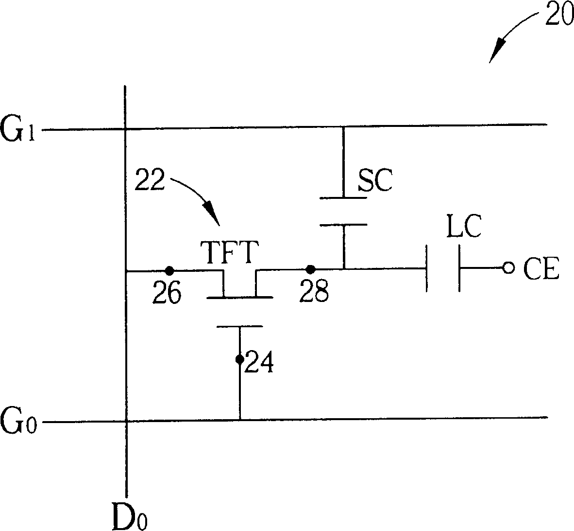
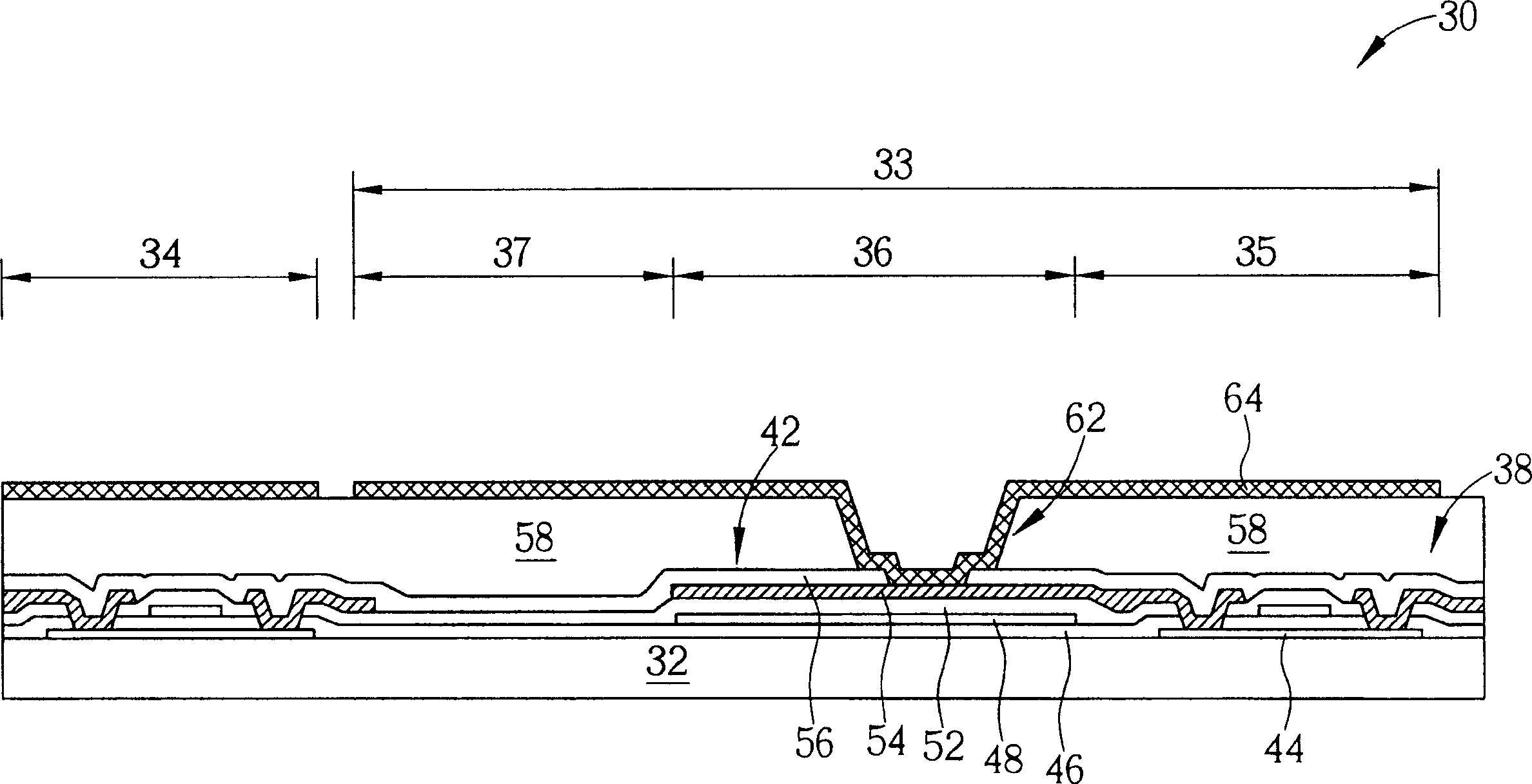
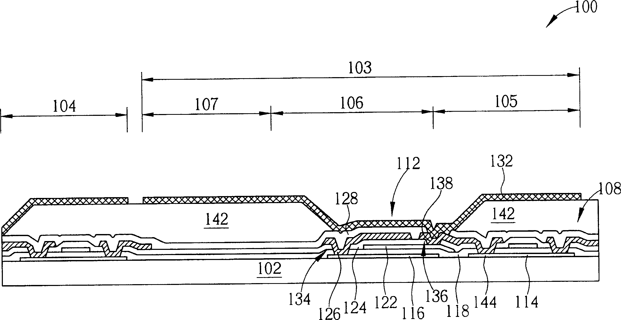
[0034] Please refer to image 3 , image 3 It is a schematic structural diagram of a thin film transistor liquid crystal display panel 100 of the present invention. Such as image 3 As shown, the thin film transistor liquid crystal display panel 100 of the present invention has a substrate 102. The substrate 102 is an insulating substrate made of a light-transmitting material, and is usually a glass substrate, a quartz substrate or a plastic substrate. The surface of the substrate 102 has a pixel array area 103 and a peripheral circuit area 104, and the pixel array area 103 also has a thin film transistor area 105 for setting a thin film transistor 108, and a capacitor area 106 for setting a storage capacitor 112 , and an opening area 107 . Since the gate 114 of the thin film transistor 108 is made of low temperature polysilicon material, the thin film transistor 107 is a low temperature polysilicon thin film transistor.

[0035] The storage capacitor 112 has a first condu...


PUM


Abstract

A capacitor structure comprises the following: first conductive layer and first insulation layer orderly located on the base plate; second conductive layer located on the first insulation layer; the second insulation layer located on second conductive layer and first insulation layer; third conductive layer located on the second insulation layer; third insulation layer located on third conductive layer and second insulation layer; the fourth conductive located on the third insulation layer. The third and fourth conductive layers are separately electrically connected with the first and second conductive layers through at least first contact hole neat the second conductive layer and at least one second contact hole.

Description

technical field [0001] The present invention relates to a capacitor (capacitor) structure, especially to a thin film transistor liquid crystal display (thin film transistor liquid crystal display, TFT-LCD) that can increase the capacitance to increase the aperture ratio. ratio) and further improve the display panel contrast (contrast) of the capacitor structure. Background technique [0002] In today's flat-panel display products, liquid crystal display (LCD) is one of the most popular technologies. For example, mobile phones, digital cameras, video cameras, notebook computers and even monitors that are common in daily life are all made of Products produced by this technology. With the improvement of people's requirements for display visual experience and the continuous expansion of new technology application fields, flat-panel displays with higher image quality, high resolution, high brightness and low price will become the trend of future display technology development. ...

Claims


Application Information

Patent Timeline
Patent Type & Authority Applications(China)
IPC IPC(8): G02F1/1345G02F1/136H01L21/00
Inventor 张志清叶光兆
Owner AU OPTRONICS CORP
Why Eureka
Try Eureka